jeffrey.kissel@LIGO.ORG - posted 19:21, Friday 28 March 2014 - last comment - 11:56, Monday 31 March 2014(11083)
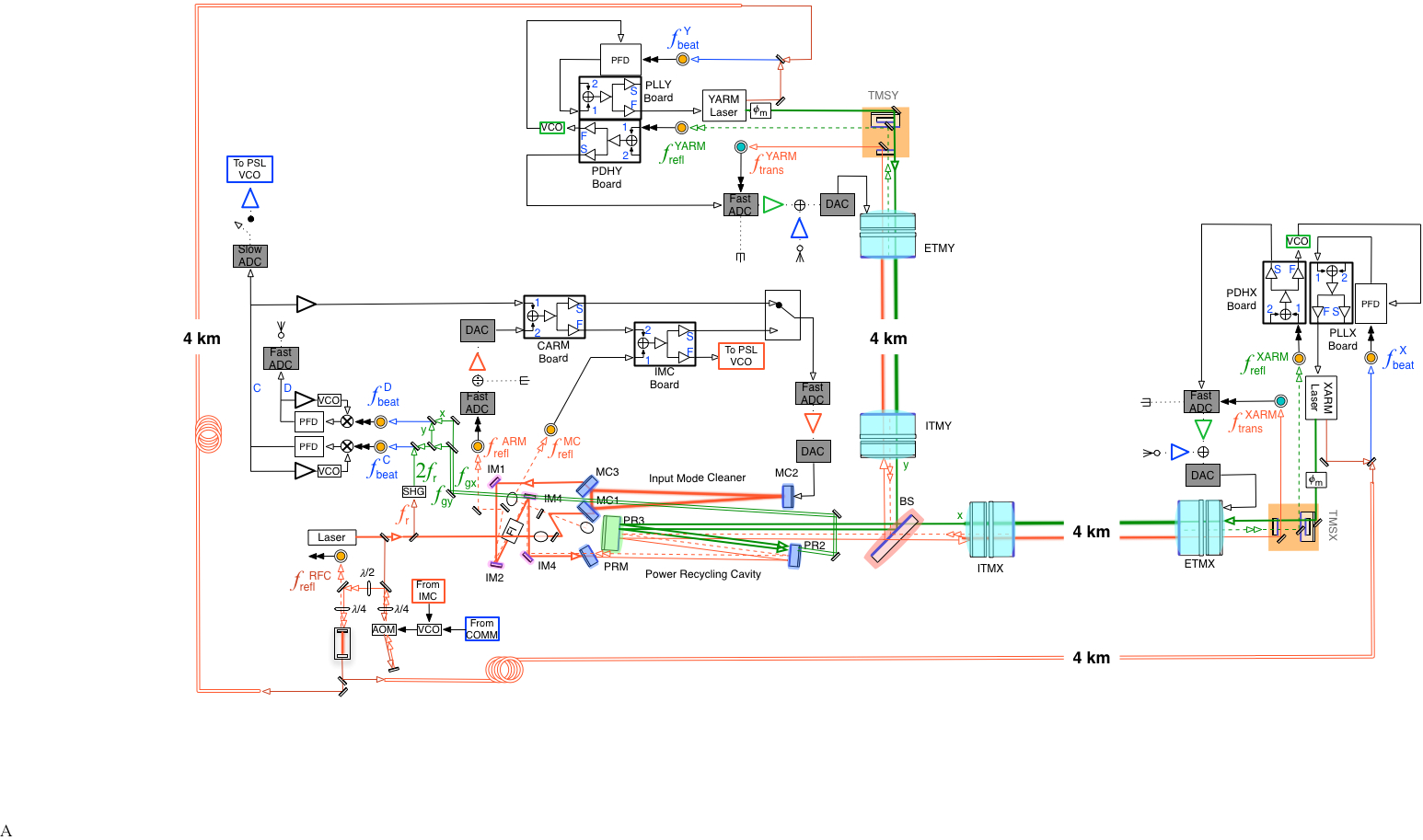
ALS Electro-optical Control Schematic
A. Staley, S. Dwyer, J. Kissel

After speaking with Sheila and Alexa, trying to understand the spectrum in LHO aLOG 11026, I realized that -- because of so much unexpected excess noise -- the current ALS setup has diverged significantly from the baseline plan. As such, we've worked together to create a diagram that is to-the-best-of-(my)-knowledge accurate, and makes sure to show how every control signal gets around to its actuators, including passes through digital land. The only things I did not include were the demodulator boards between the REFL diodes (ARM REFL, MC REFL, and the two green XARM and YARM REFLs) and lame things like whitening, AA, and AI chassis that facilitate getting in-and-out of digital land.

In particular, I draw your attention to the unorthodox and new features that were not part of the original design plan:
(1) The PRM is misaligned. This way we can use IFO REFL red diode signal (after normalizing / linearizing it with the red arm cavity trans) to measure the arm and offload at low frequency to the CARM board in the second input. This is unorthodox because normally we would feed REFL straight to the CARM board in all analog and retain the large bandwidth, but because the noise is so large, it must be linearized in the front-end (the only place the Arm TRANS signal exists), and fed out one of the corner station LSC DACs. Note that this configuration is just a special technique for these particular series of measurements and is not designed to become a normal part of the lock acquisition scheme.

(2) The Voltage Controlled Oscillator (VCO) actuated, Phase-Locking Loop (PLL) that's wrapped around the corner-station COMM and DIFF Phase-Frequency Discriminators (PFD) are used to reduce the noise enough to keep the PFD in the linear, phase detecting mode (check out pgs 6-8 of the AD9901 datasheet -- it's a really nice explanation of how it works).

(3) Before the hand-off, there's another temporary step which is to use the Beckhoff system ("Slow ADC" in the diagram) to feed directly to the PSL VCO (again at low frequency) to reduce the noise enough for the COMM hand-off to work.

This is most certainly an impressively complicated system!

Note that this diagram has been committed into the noisebudget repo here:
${NBSVN}/trunk/HIFO/Common/
and I imagine will become an "as built" DCC document in the glorious future when everything is working beautifully.
Images attached to this report
Non-image files attached to this report

Comments related to this report
Comments and my replies on the diagram from Bram, to be added/fixed later:

You are missing the Fiber Distribution Box, which shifts the laser frequency by -160 MHz before it gets shipped to the end-stations to compensate for the PSL AOM. The lasers at the end-station are then locked at the + (X-end?) and - (Y-end?) 40 MHz around the ‘0’.
Ah, yes. I had debated putting the distribution box in there, and decided against it for clarity because I forgot the important frequency shift feature.
See D1200136 for details or Figure for in T1000555 for schematical diagram.

Also, the F and S in the ‘servo’ block diagrams, is the S beckhoff?
No -- the "F" and "S" are the "Fast" and "Slow" paths of what has been traditionally called a "common mode" board everywhere -- I was trying to start a clarifying revolution with this diagram...

The lasers in the end-station get the slow temp control directly from the beckhoff from the demos error signal monitor.

The beckhoff links are a little confusing, maybe make a little color legend?