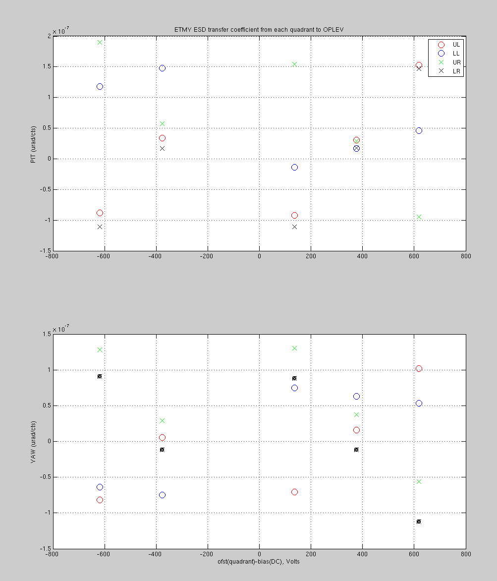
Did the same thing as X (3Hz injection to ESD each quadrant, with various offsets in DC and quadrants, measured Oplev response). And it didn't make sense (first attachment), nothing looked like a nice simple function of voltage difference.
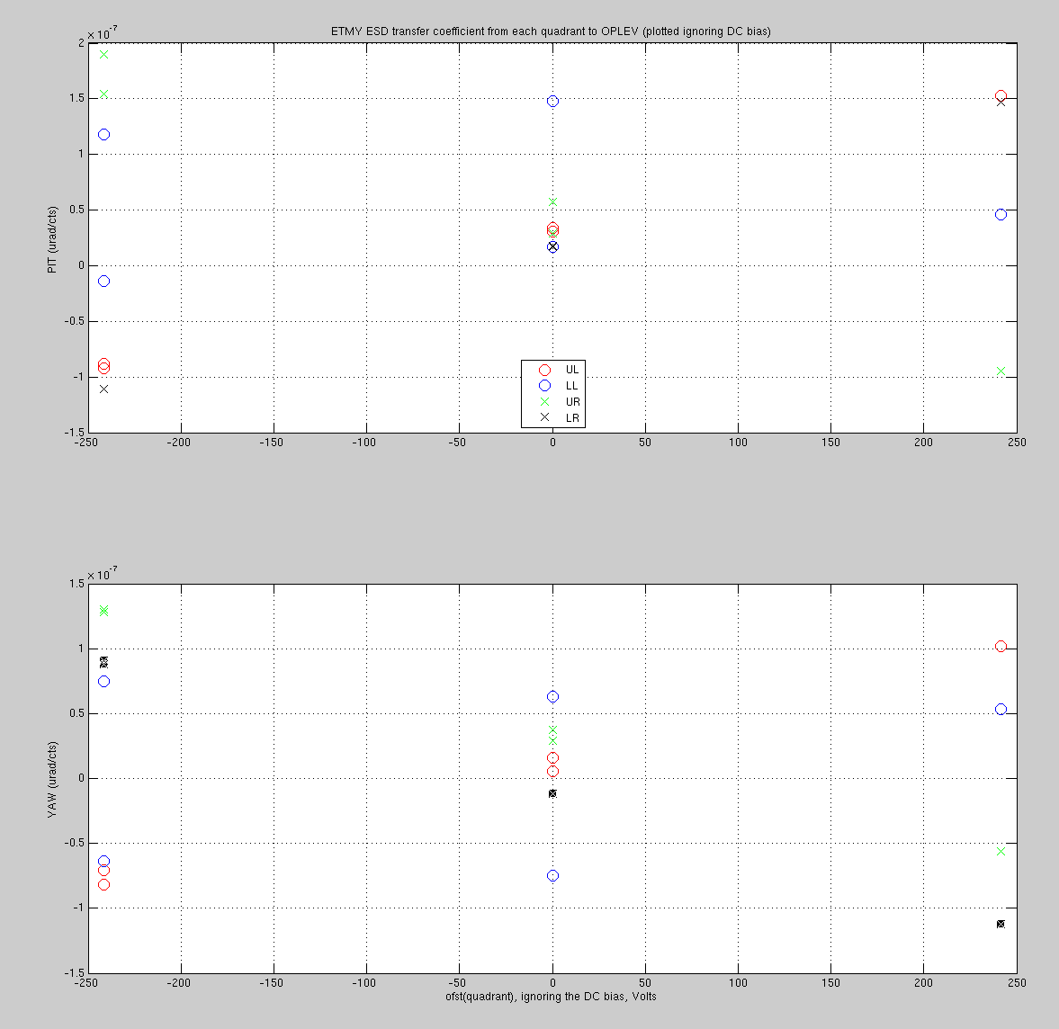
That's until you notice that at least UL, UR and LR behave as if the bias voltage stayed the same for the entire measurement. In the second plot, I used the same data as the first one but assumed that the bias stayed at zero volt, and you see that UL, UR and LR looked quite nice. The only odd thing is LL.
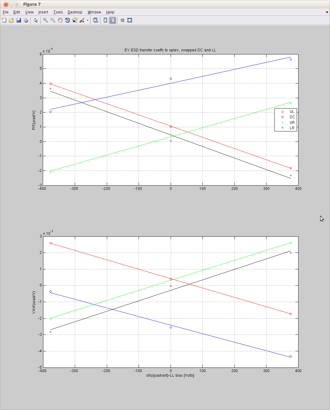
So I assumed that LL was somehow cross-wired to the DC bias. I give LL -377, 0 or 377 volt, and repeated the same measurement (I used "DC" as a replacement for LL).
This time it makes much more sense (3rd plot). Comparing it with X ESD, assuming that the oplev sign convention is the same for X and Y (which should be the case), the conclusion is that:
- LL is connected to the DC bias.
- DC is connected to UR.
- UL is connected to LR.
- UR is connected to UL.
- LR is connected to LL.
Or, if the oplev sign for P is the same but Y is the opposite of EX (which should not be the case)
- LL is connected to the DC bias.
- DC is UL.
- UL is LL.
- UR is UR.
- LR is LR.
Anyway, the effective bias voltage etc. are:
| UL | DC | UR | LR | |
| P charge effective voltage (V) | 138 | -842 | -53 | 58 |
| P slope (urad/V^2) | -7.7e-8 | 4.7e-8 | 6.2e-8 | -7.9e-8 |
| Y charge effective voltage (V) | 73 | -460 | -52 | 45 |
| Y slope (urad/V^2) | -5.7e-8 | -5.2e-8 | 6.1e-8 | 6.3e-8 |
Seems like the slopes are about the same as EX though DC is somewhat weaker.
Also, DC has a crazy offset which, if due to the charging, is equivalent of -842V (PIT) and -460V (YAW).