JasonO, KiwamuI, RickS (and RobertS, in spirit)
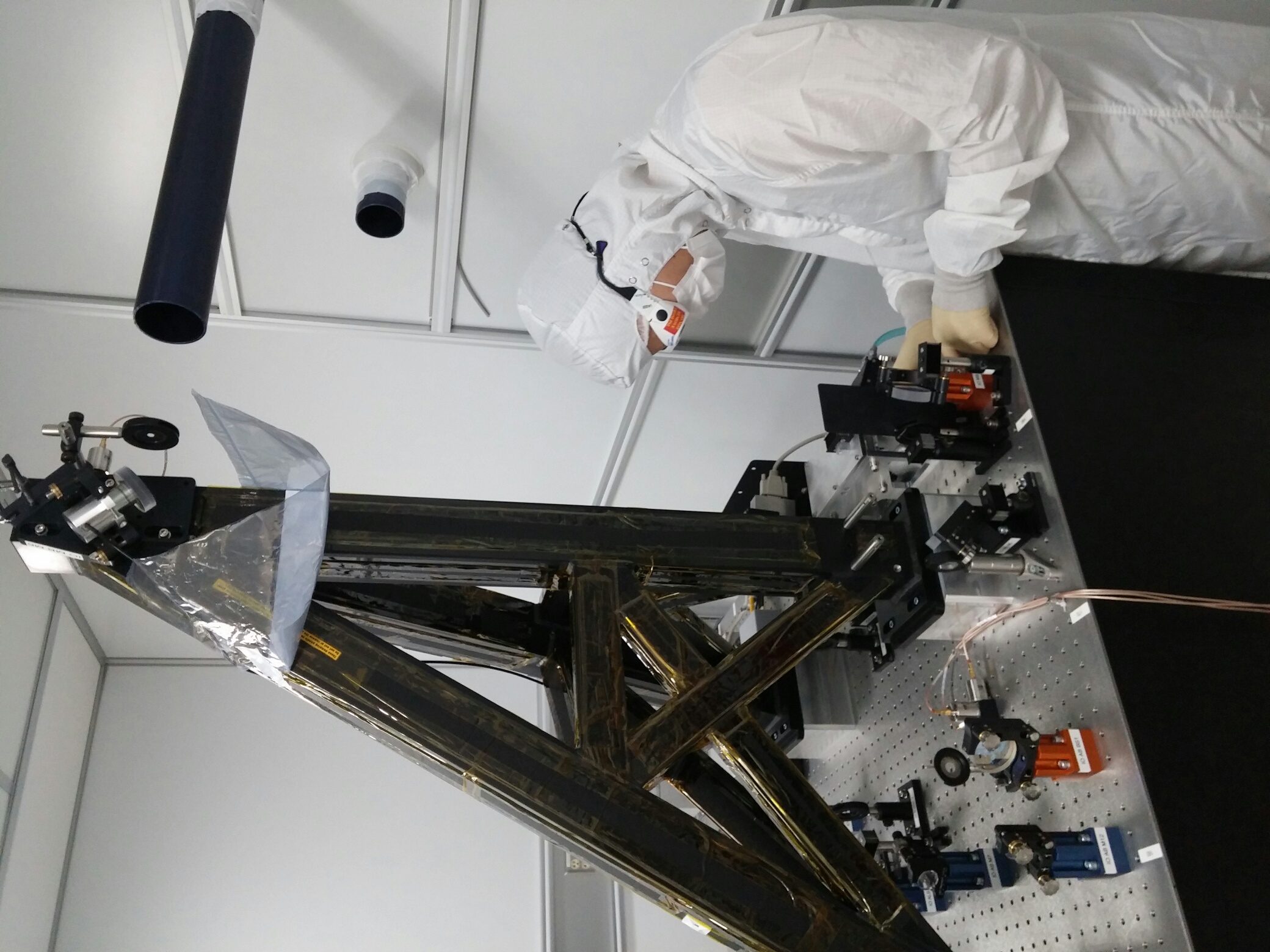
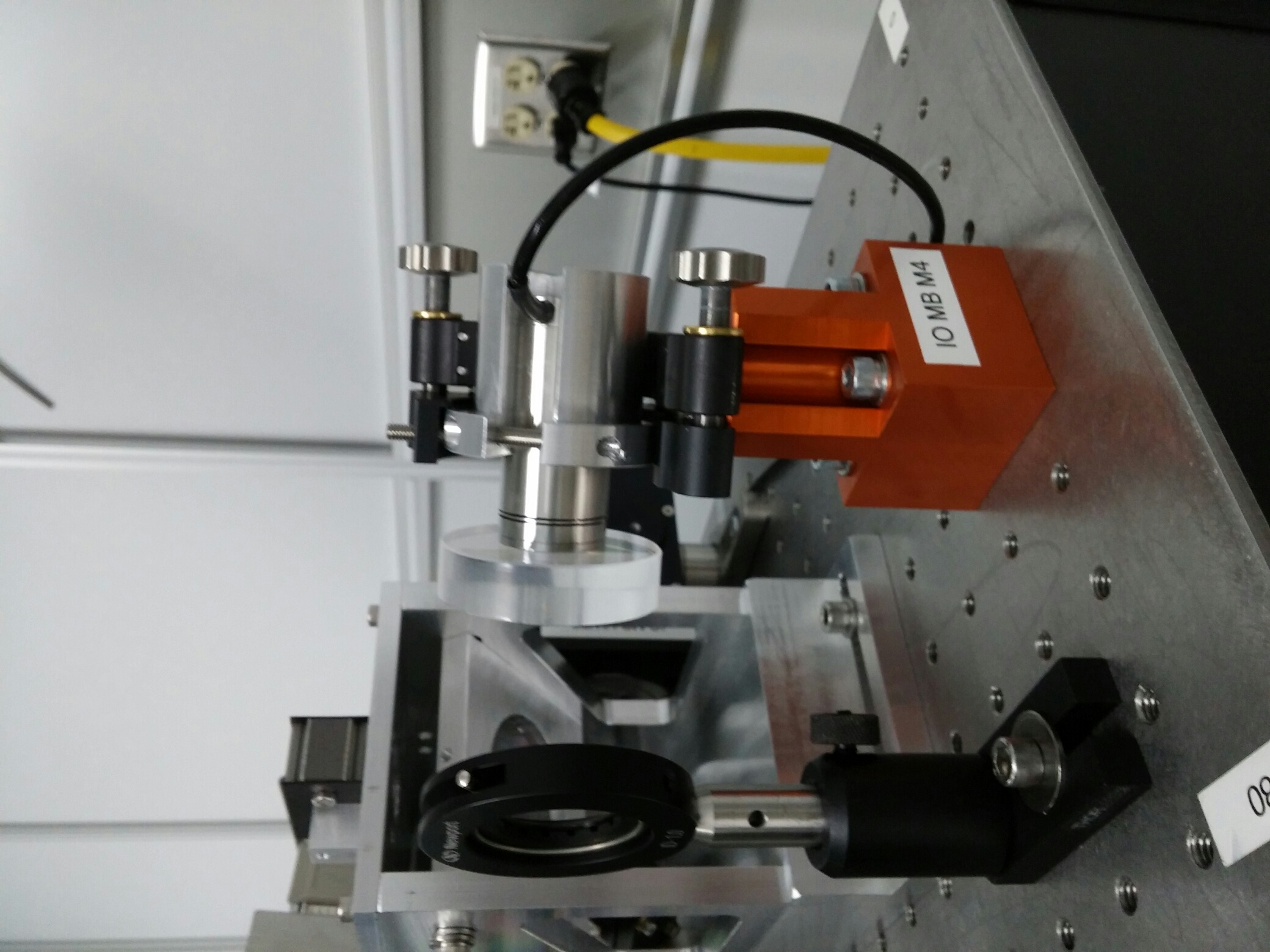
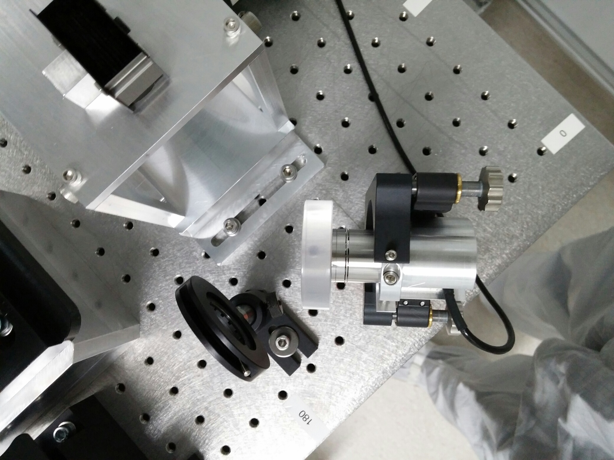
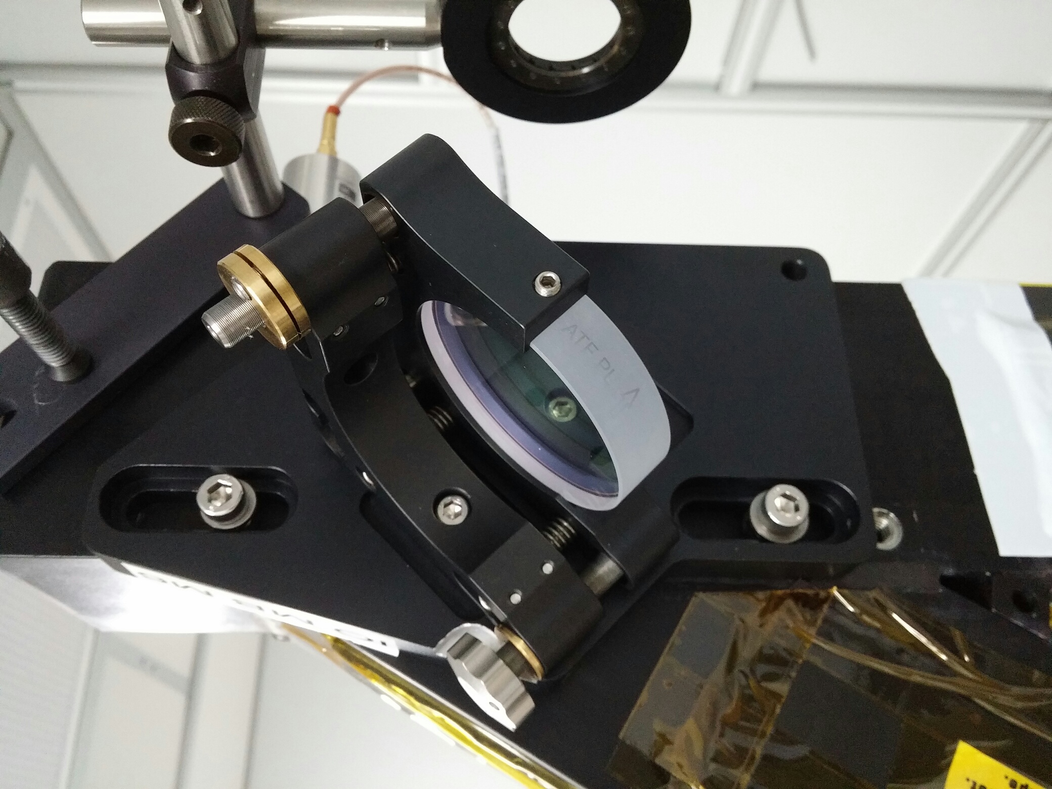
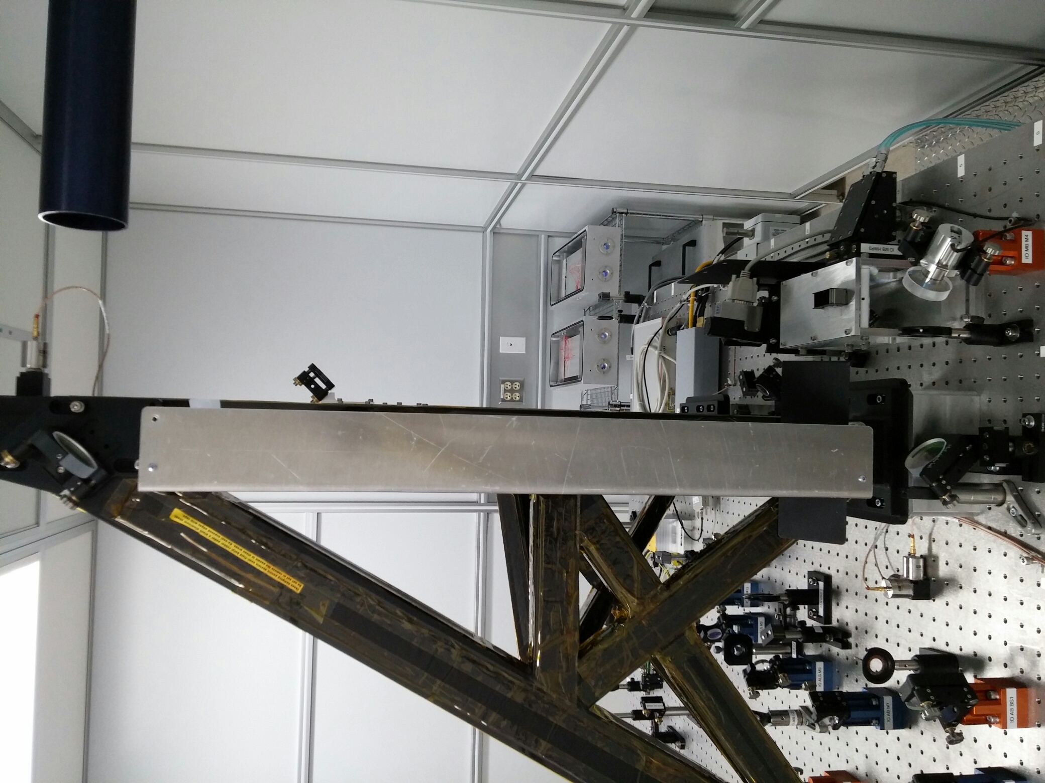
Today, we moved the PZT-controlled mirror from the top of the IO periscope down to the surface of the optical table and swapped it with with a turning mirror that was on the table. I.e. IO_MB_M6 (top of periscope) swapped with IO_MB_M4 (turning mirror immediately downstream of thin-film polarizers). Note that the PZT blocks the (weak) beam transmitted through the mirror, so we removed beam dump IO_MB_BD6.
We first installed an iris at the top mirror ouput, using a C-clamp to attach a temporary plate to the top of the periscope.
We removed the top mirror mounting plate, installed a remporary Ameristat skirt using cleanroom tape, and used a single-edge razor blade to remove some of the periscope damping material. This allowed the top plate to drop down to the required position.
We swapped the pitch actuator on the upper mirror mount to use a non-lockable actuator that doesn't interfere wtih the mounting plate.
We then used existing irises on the table in the path transmitted by the bottom periscope mirror and the iris we installed plus the spot on the outside of the PSL enclosure that reflects from the HAM1 input port to align the two mirrors we swapped.
We were able to re-install the protective shield for the vertical path up the periscope in it's original orientation.
We expect that RobertS will assess whether or not this reduced noise induced by the PZT mirror by not having it at the top of the periscope where the noise is amplified by the periscope resonance.
A few images are attached below.
Some comments from point of view of the IMC control.
-
After the pzt move, we were able to lock the IMC without an issue by just steering the top and bottom periscope mirrors by hand.
- Though we had to remove the light pipe from the shutter box (which is the one attached on the HAM1 viewport ) to coarsely check the pointing to IMC at the beginning.
- Once we locked IMC, we manually offloaded the pzt digital offsets to the mechanical knobs. As a result, now the digital offsets are less than 1000 cnts in both pitch and yaw.
- Since we mounted the pzt mirror such that it preserves the pitch and yaw relations, we did not have to introduce a funny output matrix in the IMCASC digital control.
-
We could have tuned up the output matrix for DOF_3 so as to compensate the extra lever arm length from the pzt to MC1, but we left them unchanged.
- They seem working OK anyway without any change.
-
The horizontal position of the existing beam seems to have shifted. I did not correct it for now.
- According to IM4 TRANS, beam shifted in YAW by 0.7 counts downward so that it is now -0.7 cnts.
- On the other hand the pit seems to have stayed. IM4 TRANS pit remained to be at -0.5 cnts
- This must have changed PRM spot position. We can steer one of IMs to correct it, if necessary.