Richard, Evan
Summary
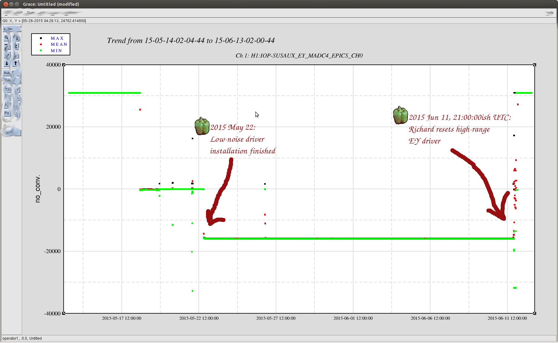
It appears that the EY ESD bias was stuck at −430 V ever since the installation of the low-voltage driver in May. It became unstuck on 11 June, when Richard reset the driver.
Since we have always requested a positive bias for EY in the digital system (using SUS-ETMY_L3_LOCK_BIAS), this means that the reset on 11 June flipped the sign of the EY ESD actuation, causing the transition of DARM from EX to EY to fail (as TJ found).
To fix the transition, the EY bias is now requested to be negative in the digital system, thereby restoring the sign (but not the magnitude) of the true analog bias that we have had since 22 May. Of course, if the magnitude of the L3 actuation has changed, this will affect the accuracy of the calibration in the region dominated by the control signal.
Details
First, let us enumerate some of the mysteries surrounding the EY ESD:
- After the low-voltage driver was installed (i.e., after 2015-05-22), we found that we had to flip the sign of the L3 actuation from positive to negative. This is despite the fact that both the low-voltage driver and the high-range driver supposedly have positive polarity at dc (so we should not expect to have to compensate for an analog sign flip).
- After the low-voltage driver was installed, we found that the dc actuation strength of EY L3 was 50 times weaker than EX L3. We expect only a factor of 20×1.25 = 25. The factor of 20 comes from the difference in dc gain between the high-range driver and the low-noise driver (40 V/V versus 2 V/V). The factor of 1.25 is what Kiwamu had previously found necessary to match the dc strengths of EX L3 and EY L3 when they were both driven by the high-range drivers.
- After the low-voltage driver was installed, the analog readbacks for the high-range driver (bias line and 4 quadrants) were stuck at −15000 ct.
- After Richard reset the high-range EY driver for the charge measurements (2015-06-11, circa 21:00:00 UTC), there has not been a successful transition of DARM from EX to EY (although there have been only four trials, according to the summary pages).
We hypothesize that mysteries (1), (3), and (4) are explained by the EY ESD bias being stuck at −430 V between 2015-05-22 and 2015-06-11, and the driver's readbacks being nonresponsive. Mystery 2 is still unsolved.
When Richard went to EY on the 11th, he found the high-range driver putting out −430 V on all five lines, and the driver's analog readbacks were frozen at −15000 ct or so. According to him, this is a known failure mode of the driver's microcontroller. After he reset the driver, the analog readbacks became functional again.
The attached plot shows a trend of the analog readback of the EY ESD bias. It is stuck at about −15000 ct from 2015-05-22 (when the low-voltage driver installation was finished) to 2016-06-11 21:00:00ish UTC (when Richard reset the driver). The natural conclusion from this is that the EY ESD bias has been railed at −430 V between these two dates (even though we thought we were giving +380 V of bias).
I flipped the requested bias so that it is now (I think) −380 V, which is the most negative bias that can be requested from the driver when it is operating properly. I was able to transition control of DARM from EX to EY by hand following the steps in the guardian.
Also, Travis and I are hearing ETMY saturations every so often. The rms drive to EY L2 is 40000 ct or so, which is higher than the 15000 ct that we measured when we first started using EY L2. (Could it just be wind?)
If you, like us, don't like it when your suspensions saturate in full lock, then we suggest trying out a higher L1/L2 crossover. Engage FM9 in H1:SUS-ETMY_L1_LOCK_L, and turn up the gain from 0.16 to 0.31.
Per Jeff's request, here is an excerpt from an email I sent to Evan and Jeff:

Some architectures used in amplifiers suffer from a phenomenon known as Phase Reversal wherein the feedback sign of the amplifier can actually change on certain saturation events.  I have not looked to see if that is whatsoever possible with the HV ESD amplifiers.

Something that bothers me here is that if you are running in low voltage mode, there is no way the high voltage drive signals for the quadrants can make it to the reaction mass.  A relay disconnects them.  This makes me somewhat puzzled about potential HV/LV interactions causing any sort of actuation force reduction.  The actual applied bias could be changing by the time it makes it through the non-trivial series resistance associated with the bias filters (~70kohms), but there would have to be a low impedance on the bias terminal to created the necessary voltage divider.

As for the sign flip, I have no answer there.  I will check (again) that I didn't do something dumb and make a typo on the + and - wires.
Following up on the notion of phase reversal, I checked all the chips used in the HV ESD Driver signal chain.  Here's the result:

LT1124 - Input receiver, these are the same architecture as the ubiquitous LT1125 we use everywhere at LIGO, so I'm not too suspicious here.
LT1007 - Second stage of input receiver, no mention of immunity to phase reversal in data sheet.  This is often a bragging point among chip designers, so I can't eliminate this chip from the list of suspects.
OP-97 - Front end chip for the HV output stage, Vcm = +/-13.5V min, this is a possible culprit as the input architecture appears to be jfet based, and it's used in a feedback loop, which is a double whammy for phase reversal.
PA-95 - HV driver chip.  No mention of phase reversal immunity.  Definitely jfet based, used in a feedback loop, and is not grounded on the positive pin.  Triple whammy for phase reversal, although it would be hard to exceed the input common mode voltage with +/-430V rails...

Mostly pseudo science here, but my two cents.