The new prototype board was modified to satisfy some of the things in the requirement (T1600064) as listed in 1., 3. and 5. below. I also listed things that were not modified but would have been good if recommendations in T1600064 were implemented.
I wouldn't claim that we won't modify it further, but this is just the current state.
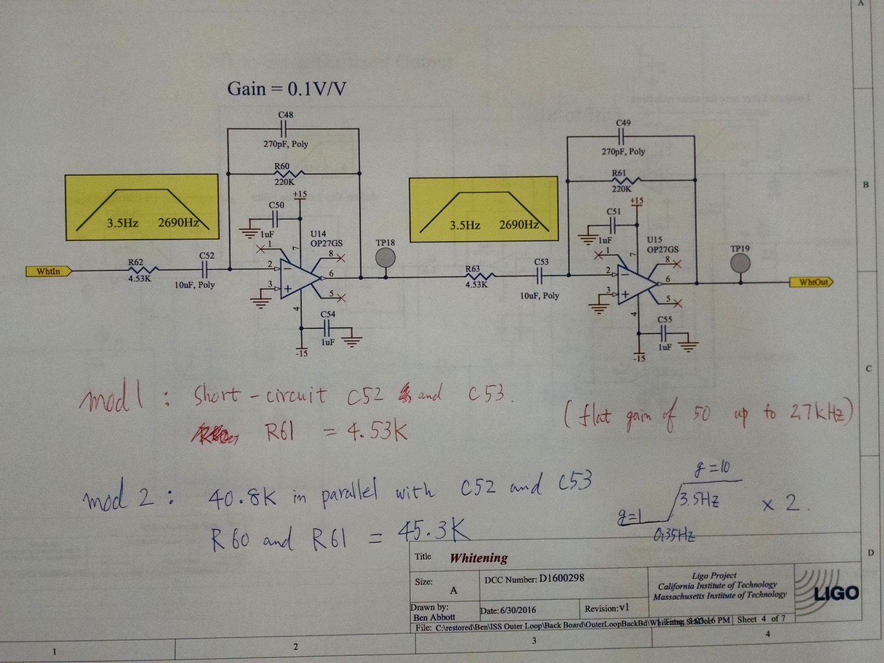
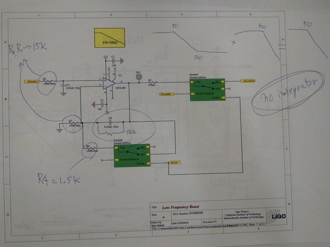
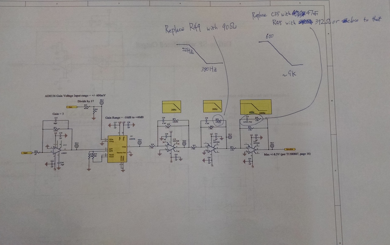
In this entry you'll be able to see the electronics modifications in the attached, but the photos are too small to read the original component values, so read the original drawing D1600298 as necessary.
1. Readback of the PD array signal after the servo loop switch ("SUM PE MON") needed to be DC coupled.
The "whitening" was originally AC-coupled (second attachment) and therefore it was not compatible with digital AC coupling described in the requirement.
We bypassed the big caps in the input of the opamps with some resistors so it acts as one single pole at 2.7k with DC gain of 50 (second attachment, mod 1).
To make the OLTF measurement easier, we made the same change to the whitening downstream of the summation for the excitation DAC output.
The servo board output readback was also AC-coupled, but we want to see if everything is working fine including DC injected into the inner loop board.
We made the output whitening a true whitening (second attachment, mod 2). 0.35Hz zero might be too low, though.
2. The board doesn't implement the analog compensation for the in the inner loop filtering upstream of the error point.
The inner loop error point "whitening" works as a very steep boost seen from the outer loop, roughly an equivalent of (z, p) = ([3; 3; 130], [0.07, 0.07]). T1600064 reccomends to implement the same thing in the outer loop somewhere to cancel this effect to make the loop design simpler.
Since this is not compensated in the prototype board, the outer loop OLTF would become huge for f<3Hz. This means that the digital AC coupling servo should work REALLY hard to effectively AC-couple the entire outer loop at, say, f<1Hz, without reducing the outer loop gain at 10Hz and up.
We do not implement this by analog cut and paste job (no opeamp available for this on the board), but we'll try to make it work by an aggressive digital AC-coupling filter.
3. Integrator as a boost doesn't go well with digital AC coupling so it was converted to a usual boost with finite DC gain.
The error point of the digital AC coupling servo is kept zero at DC (i.e. a pole at zero Hz). The outer loop prototype had an integrator as a boost.
Of course they don't go well as any tiny DC difference between the AC coupling error point and the integrator input will be integrated and eventually the servo runs away. But we don't really need a pole at zero Hz.
We changed it such that the first boost acts as 50Hz LPF with DC gain of 10, and when added to a flat unity gain it becomes 500:50 boost (third attachment) (but see the next entry).
4. Boosts were implemented as three parallel integrators added to a flat unity gain.
We had a choice of unity gain, zp=50:0, 100:0 or 150:0. See the first and the third attachment.
As described in 3. above, we already changed one integrator to []:50 LPF so the boost becomes 500:50.
We didn't fix the parallel summation, it might be OK to go without any boost or using just one.
But T1600064 shows our standard practice of connecting boosts in series.
5. Outer loop servo filters on the board were also changed.
Originally the servo filtering was something like (z,p)=(100, [20^2;40]) (fourth attachment). As described in 2. above, 1st loop effectively adds ([3^2; 130], [0.07^2]). IMC adds another pole at ~8kHz.
Everything added together it's like ([3^2; 100; 130], [0.07^2; 20^2; 40; 8k]), and this might be OK.
But we made a change so the board became ([380;9k],[20^2;600]) by changing one of zero-Ohm resistors in the second stage and one C-R pair in the third stage (fourth attachment). Everything added together it would be ([3^2;130;380;9k], [0.07^2; 20^2;600; 8k]).
This change might not have been necessary. We just felt that letting a big 4.7uF capacitor and a zero-Ohm resistor to determine AC gain at around 10kHz in the first as well as the second stage was maybe too much of an uncertainty in the AC gain.
6. Sallen-Key at 0.1Hz for Digital AC coupling path might be too aggressive
For the moment the Sallen-Key is disabled for the digital AC coupling path (so the only analog filtering is a 10Hz LPF) to make things easier as we try to make it work.
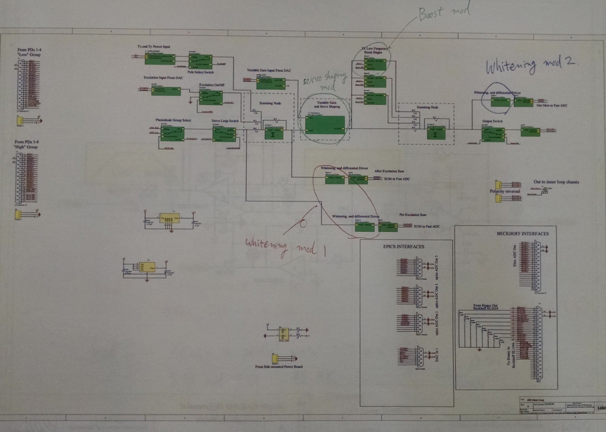
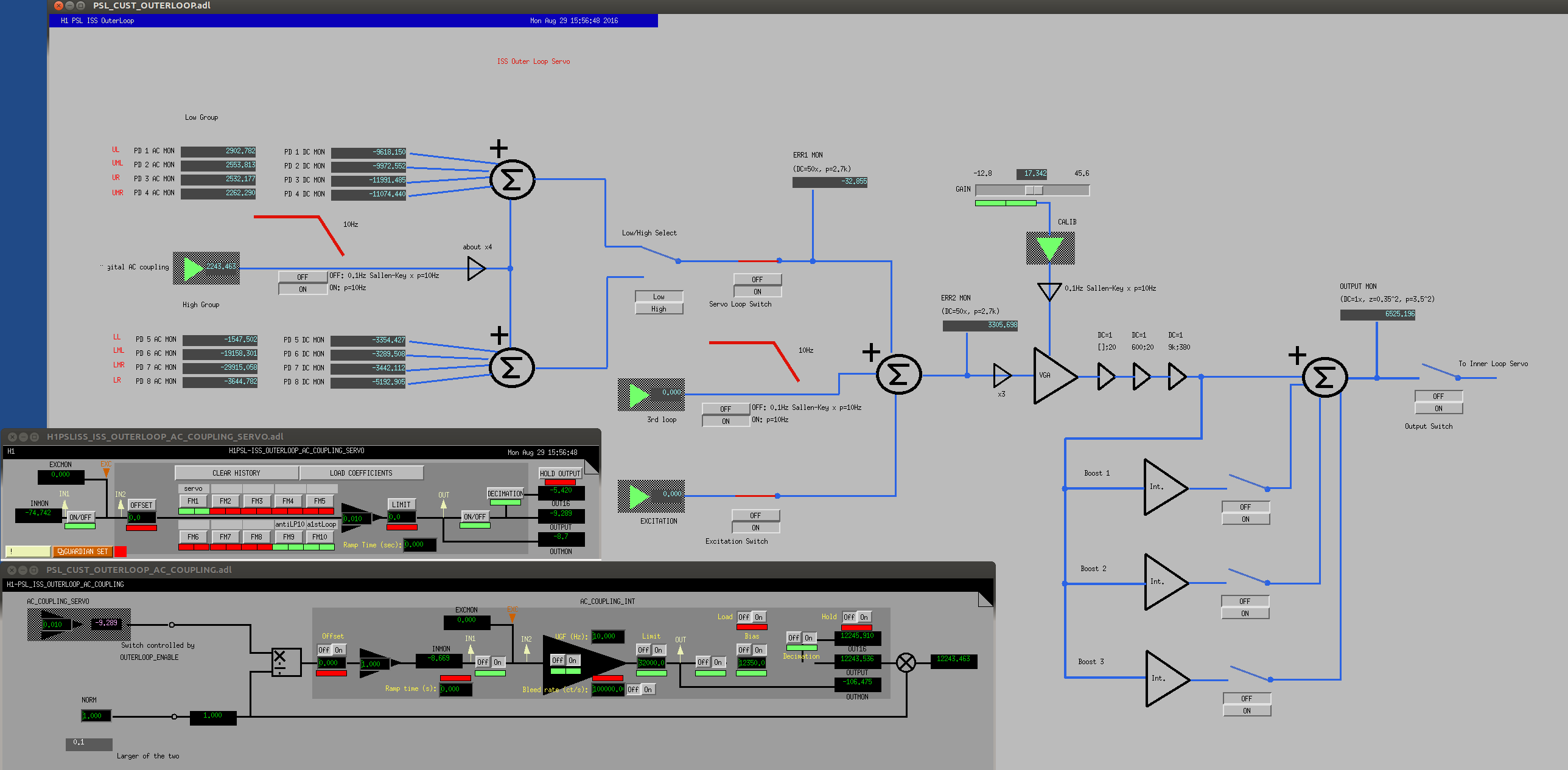
Outer loop and digital AC coupling topology
Error point for the digital AC coupling is upstream of the summation point for the outer loop and the third loop (ERR1 in the attached medm). This comes from two requirements:
- AC coupling is strong enough so the outer loop survives the power up. This means that the outer loop lower UGF is in effect somewhere between 0.1Hz and 1Hz, and the AC coupling OLTF needs to be huge at that frequency.
- 3rd loop needs to suppress the intensity at 0.7Hz or so.
If the error point is downstream, the 3rd loop gain will be eaten by the AC coupling loop.
This means that, as we change the VGA gain, the offset coming between the AC coupling error point and the input to the VGA will be amplified and injected downstream, and if this becomes the problem we need to compensate for that using the analog excitation offset.
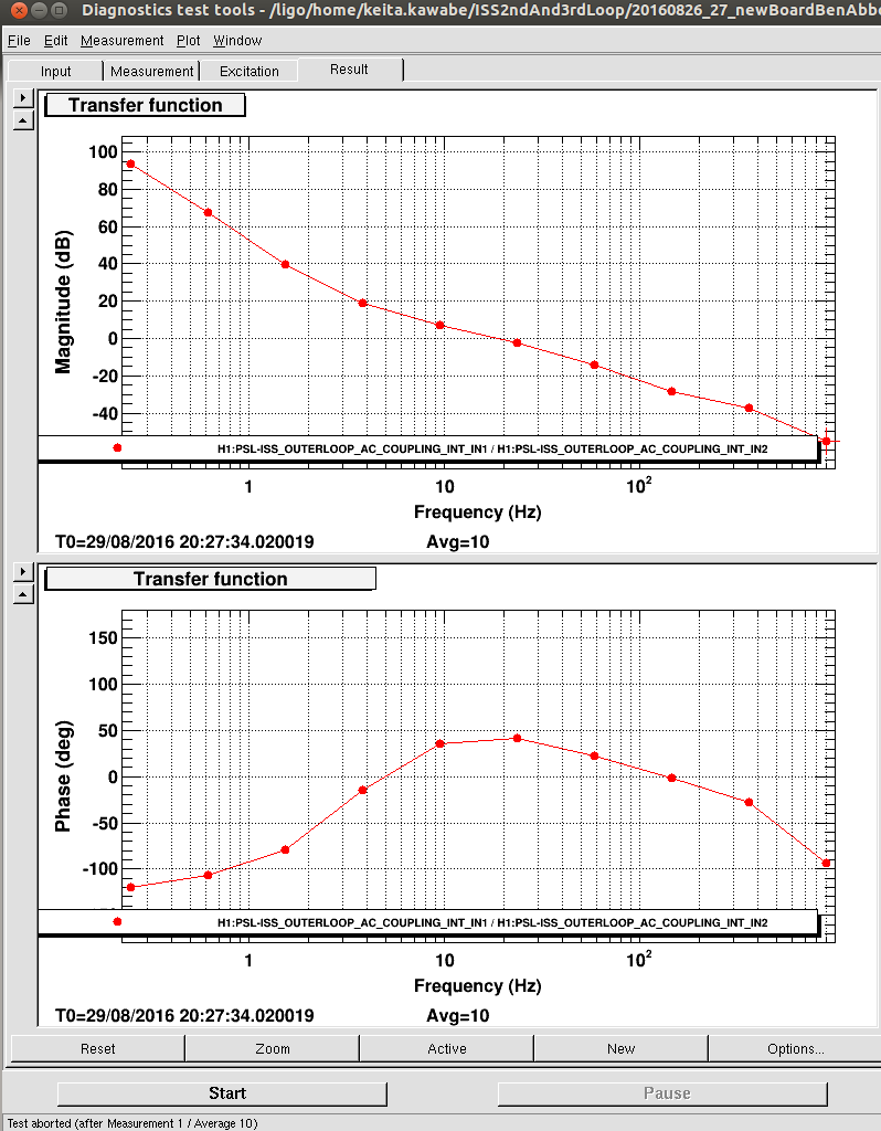
Second attachment shows the AC coupling OLTF, with the setting shown in the first attachment.
I was looking (again) at the ISS inner loop circuit diagram to make sure that I understand the system correctly and found that my alog 26879 was wrong about inner loop diode in that one pole and one zero were somehow swapped (see the new entry I've just made as an attachment to the alog 26879.
Anyway, since the amplitude actuation of the outer loop summation point of the inner loop is the inverse of the inner loop sensing "whitening", 2. should read
"The inner loop error point "whitening" works as a very steep boost seen from the outer loop, roughly an equivalent of (z, p) = ([3; 3; 2.34k;2.7k], [0.07;0.07;130])".
Sorry for a confusion, it seems like it's too late to fix the original alog entry above.
Correction of correction (sorry).
Original alog 26879 seems to have been correct, therefore the origial entry of this alog should be correct.
The inner loop error point "whitening" works as a very steep boost seen from the outer loop, roughly an equivalent of (z,p)=([3; 3; 130], [0.07, 0.07])
Sorry for further confusion. Again I cannot correct the above original entry nor the above correction any more, thus this entry.