M. Pirello
Prior to working on this we determined that the analog voltages on the channels in questions are outputting anticipated values. The immediate problem is with the PowerOK bit for each of these signals.
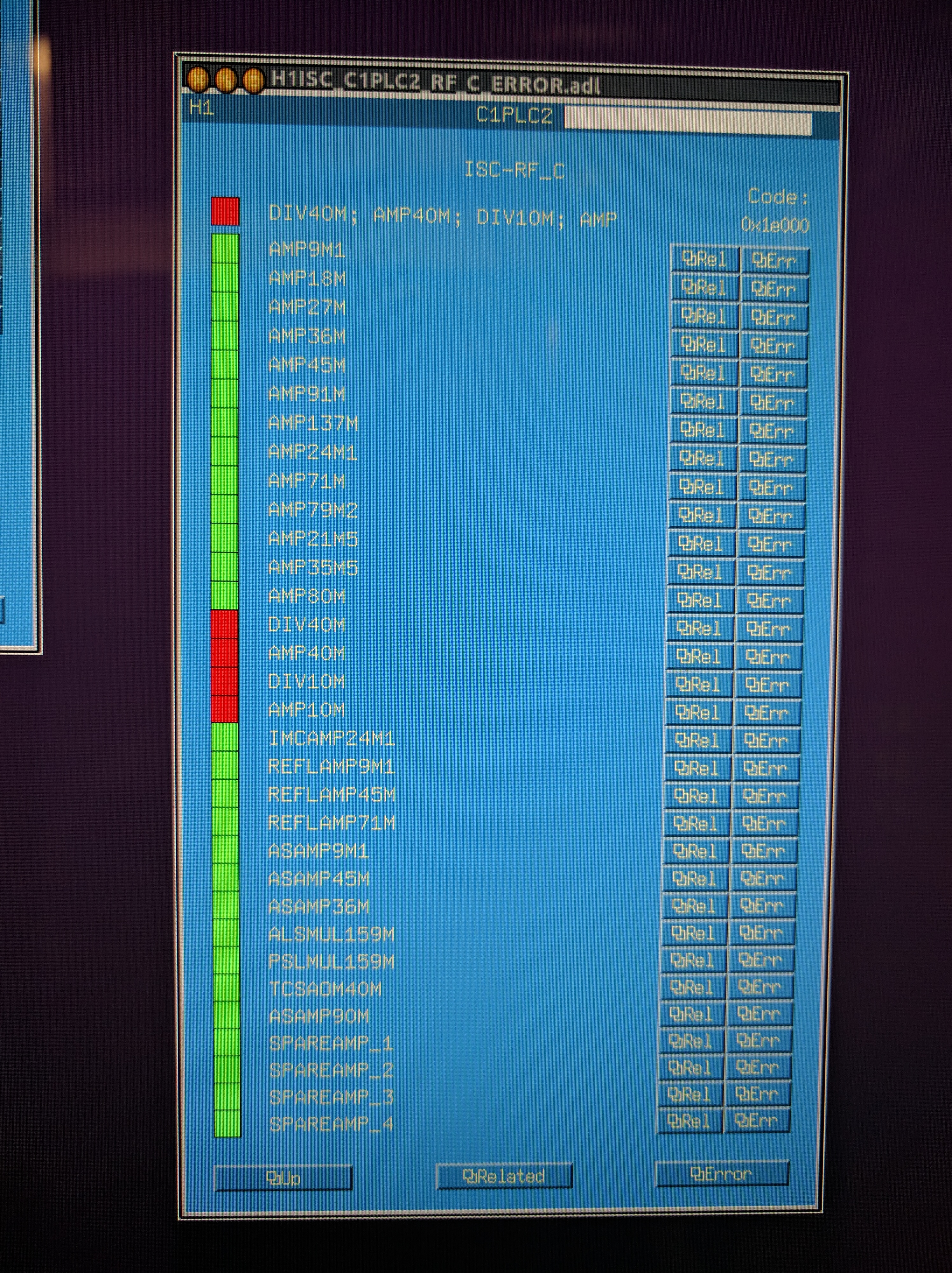
Investigation into these chassis yeilded the following:
1. Upon rebooting RF Amp Concentrator #1 on ISC_C3 in the CER (S1103450) the stuck bits on that chassis AMP18M and AMP24M1 were reset. We are 2/3 of the way done with this task, piece of cake!
2. Upon rebooting RF Amp Concentrator #2 on ISC_C3 in the CER (S1103451) 3 new bits were stuck for a total of 4 bits, including the original DIV40M, drat!
3. I tried disconnecting, measuring, and reconnecting each of the 4 stuck signals on the DB25's on the back of the unit. These voltages look good, no luck resetting the latched bits here.
a. DB25#1 = DIV40M = 3.64V
b. DB25#2 = AMP40M = 3.75V
c. DB25#3 = DIV10M = 3.61V
d. DB25#4 = AMP10M = 3.67V
4. I then disconnected the DB37 on RF Amp Concentrator #2 (S1103451) and checked each signal coming out of the RF Amp Concentrator. This output is confusing. The I couplers inside are referenced to 5V. An on state should be 5V, off state should be 0V. All of the PO signals should be either 5V or 0V. PO11 is 2.5V, PO7 is 2.5V, PO2 is 2.5V.
| PIn 1 (M1P12) | 0V | Pin 11 (M1P2) | 0V | Pin 21 (M1N11) | 0.033V | Pin 31 (M1N1) | 0.004V |
| Pin 2 (M1P11) | 0V | Pin 12 (M1P1) | 0V | Pin 22 (M1N10) | 0.029V | Pin 32 (PO8) | 0.009V |
| Pin 3 (M1P10) | 3.4V | Pin 13 (PO12) | 0.008V | Pin 23 (M1N9) | 0.029V | Pin 33 (PO11) | 2.509V |
| Pin 4 (M1P9) | 2.598V | Pin 14 (PO4) | 0.008V | Pin 24 (M1N8) | 0.0228V | Pin 34 (PO3) | 0.005V |
| Pin 5 (M1P8) | 0V | Pin 15 (PO7) | 2.510V | Pin 25 (M1N7) | 0.002V | Pin 35 (PO6) | 0.006V |
| Pin 6 (M1P7) | 2.951V | Pin 16 (PO10) | 0.007 | Pin 26 (M1N6) | 0.033V | Pin 36 (PO9) | 0.004V |
| Pin 7 (M1P6) | 3.073V | Pin 17 (PO2) | 2.515V | Pin 27 (M1N5) | 0.033V | Pin 37 (PO1) | 0.003V |
| Pin 8 (M1P5) | 3.027V | Pin 18 (PO5) | 0.004V | Pin 28 (M1N4) | 0.005V | ||
| Pin 9 (M1P4) | 3.051V | Pin 19 (GND) | GND | Pin 29 (M1N3) | 0.004V | ||
| Pin 10 (M1P3) | 0V | Pin 20 (M1N12) | 0.029V | Pin 30 (M1N2) | 0.004V |
5. I then reconnected the DB37 to H1_EtherCAT_Corner_3. Ten out of twelve of the OK bits remained red. I recycled power on the RF Amp Concentrator #2 (S1103451) on ISC_3 and again all but 4 of the OK bits were green like before.
6. I put everything back together, removed the breakout boards, etc. When I left the CER, the 4 bits were latched, DIV40M, AMP40M, DIV10M, AMP10M. After noon I checked the OK bits and 10 out of 12 OK bits are red including the original four. I am relatively sure that the issue is with the RF Amp Concentrator. The power OK signals going into this chassis are good, the power OK signals coming out of it seem to latch up spontaneously and output bad voltages. Perhaps the 5V regulator is outputting 2.5V?
Recommendation:
Strike DIV40M from WP6248 and close out WP6248 and FRS 6391 because DIV40M is connected to a different chassis. Expand FRS 6059 to encompass RF Amp Concentrator #2 (S1103451) and work to debug the source of the spontaneous latchup/latchdown and bad voltages (including DIV40M).