This is an update on my previous entry 46952.
Field content
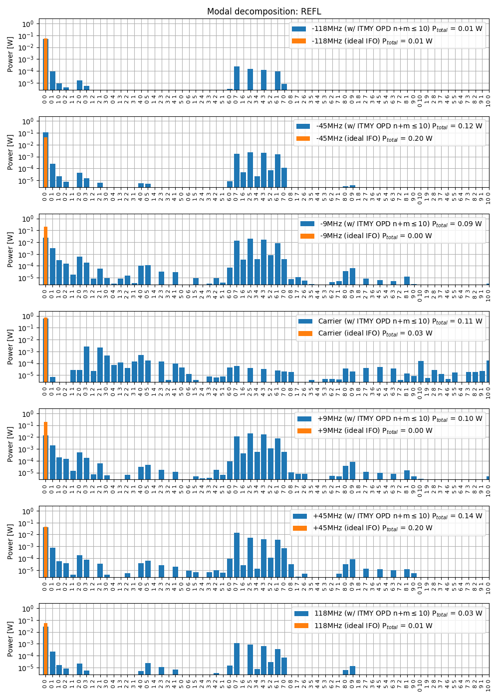
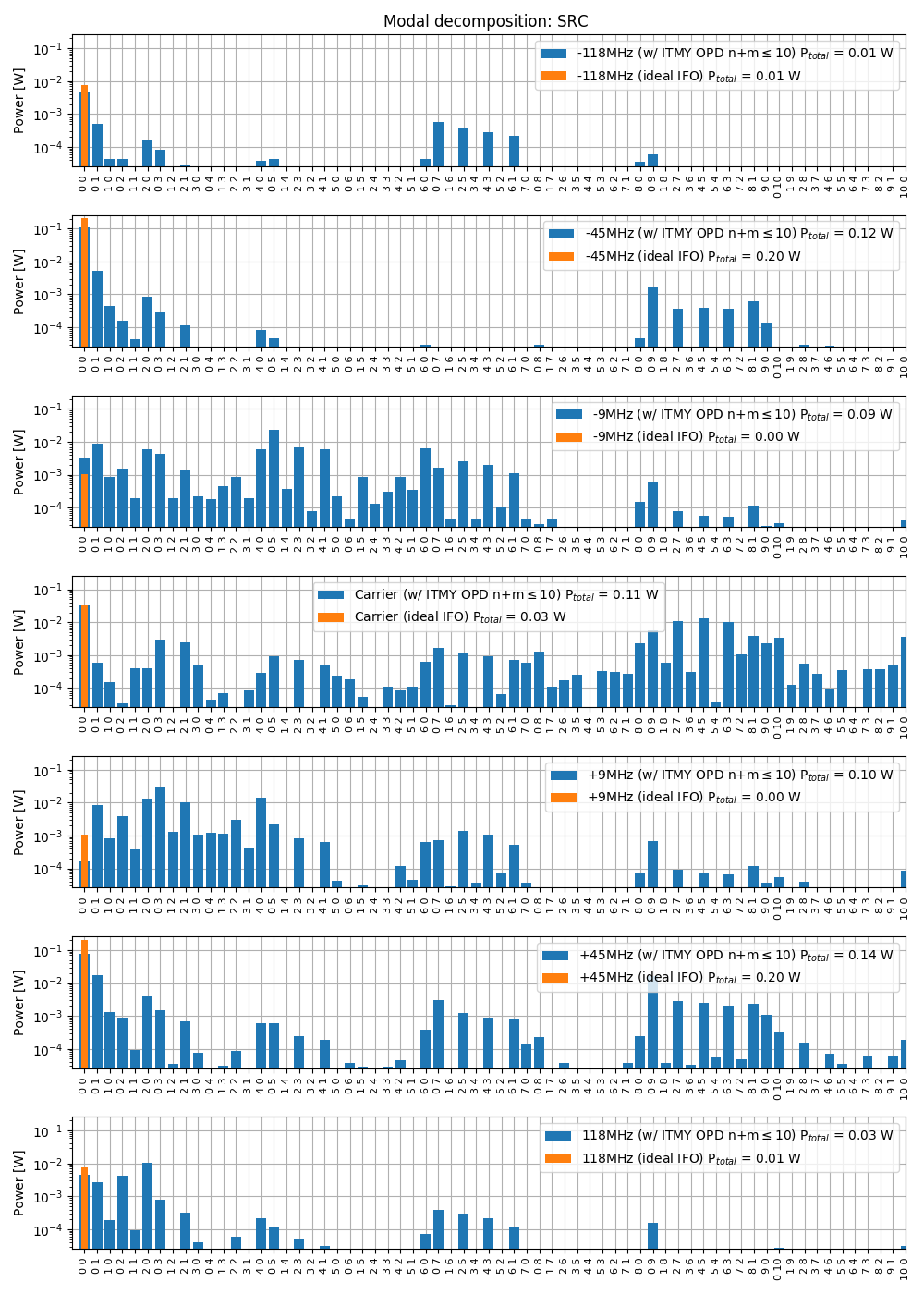
Using the optical path distortion measured by the HWS (provided by Aidan, see also 46127 and 46888) I simulated the mode content at various ports in a dual recycled Fabry-Perot Michelson interferometer. The simulation is done with MIST, using Hermite Gauss modes up to order 10, and locking the interferometer using simulated error signals. In the original entry 46952, the path distortion was about half of what we expect at 26 W (because the wavefront map provide by Aidan corresponds to a power step of about 15 W). So in the results considered here I multiplied the map by two.
Only the optical path distortion in the ITM is included, there is no deformation of the HR surface.
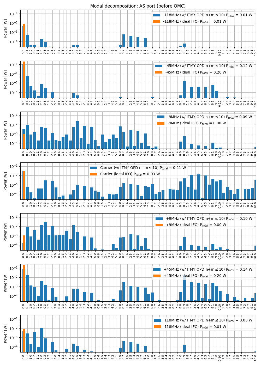
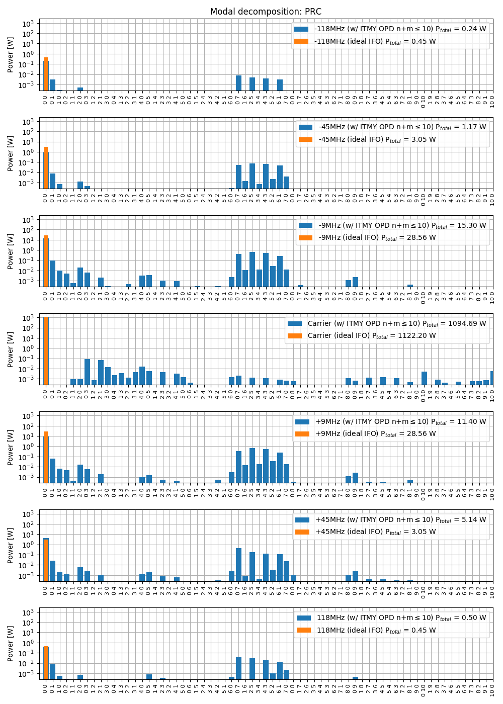
Each of the attached plots show the distribution of power into each modes, assuming 26 W of input power, 60ppm or round trip losses per arm. The orange traces are there for comparison, to show that in a ideal IFO, all power is in the fundamental TEM00 mode.
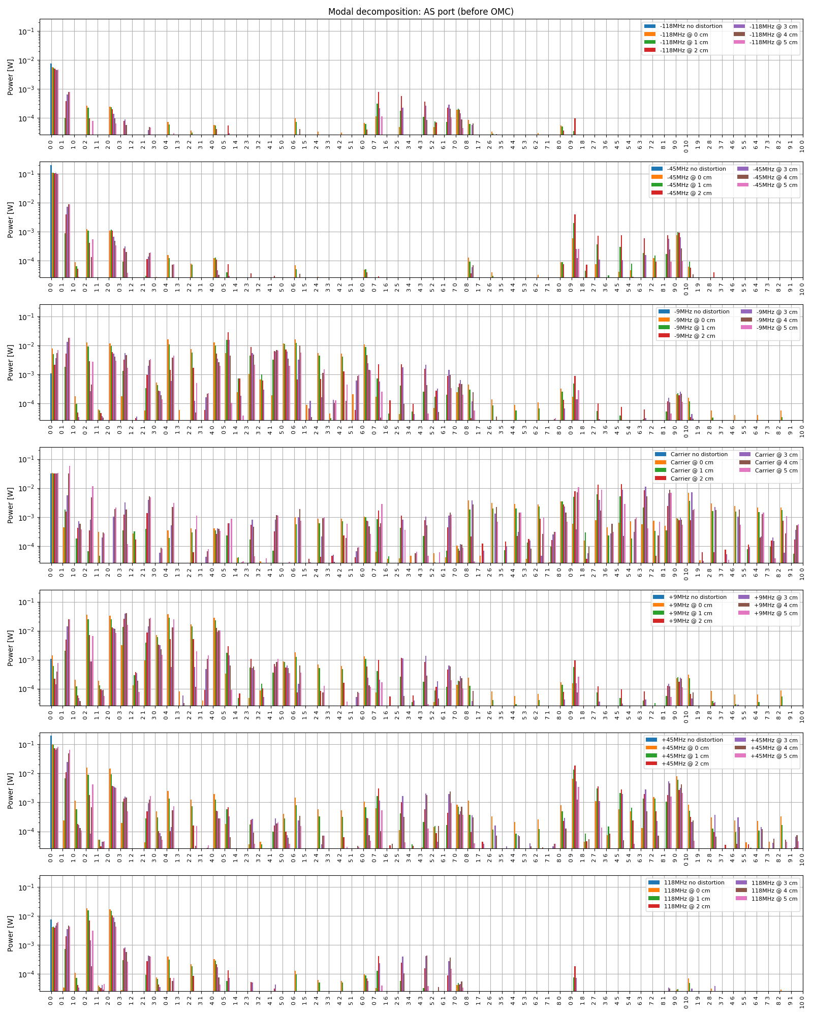
Interestingly, the point absorber seems to create some 9MHz sideband power in modes of order 9 at the AS port, which we believe are the culprit for the high RF9 modulation noise coupling.
RIN coupling
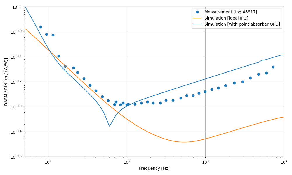
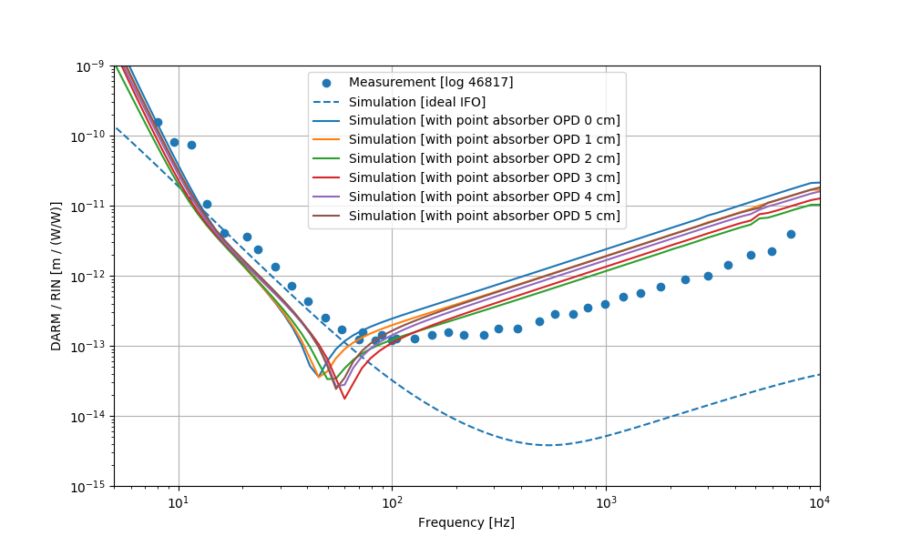
Using the same simulation described above, I could compute the coupling of input RIN to DARM. The result is shown below, compared with Craig's measurement from 46817. The distortion produced by the point absorber seems to explain qualitatively (even though not quantitatively) the increased coupling at high frequency. The magnitude of the coupling is larger in simulation, but roughly ok. The coupling scales with the amplitude of the optical path distortion, and it's likely to change if the point absorber is moved by a cm or two, probably within the uncertainty of the beam center position in the HWS map.
Sidebands RIN
According to the simulation, there is about 1 mW of 9MHz sidebands power in the modes of order 9. Assuming that all of this mode is transmitted through the OMC, we can compute the DARM noise corresponding to sideband RIN:
DARM = SB_RIN * SB_POWER / (OMC_DC / DARM)
From 46985 I estimate a DARM noise at a level of DARM ~= 5e-20 m/rHz at 100 Hz. From the simulation I have OMC_DC / DARM ~= 1.2e10 W/m, from which
SB_RIN ~= 4e-7 /rHz
is the level of 9 MHz sidebands RIN that would explain the DARM noise, assuming it's all due to RF9 TEM9 mode leakage.
The position of the point absorber has, as expected, an effect on the simulation results. Here I started by centering the peak of the optical path distortion (OPD) at the center of the beam, and then move it to the side by steps os 1 cm, up to 5 cm from the center. I maintained the same peak amplitude of the OPD, so the shift does not take into account the change in the power that is actually absorbed. This simulation is just to get a feeling of how much the results change because of the uncertainty of the beam center position w.r.t. to the HWS frame.
The first plot shows that the coupling of RIN to DARM changes a bit, but not much, with the absorber position.
The second plot shows the mode content at the AS portfor the different positions. I realize this is a busy plot and hard to get much information out of it. I'll try to find a better representation soon.
CAVEAT: in all the simulations reported so far, I have included only the point absorber map on the ITMY substrate. To have a more realistic simulation, I should include the intrinsic and thermal lenses in both ITMs, as well as the effect of Ring Heaters and CO2 laser. Working on it.
Updates
- included thermal, static, CO2 and RH lenses as described by Aidan in 47060
- when using the ITMY map with the correct amplitude, the simulation was not able to properly lock using the error signals. It turns out that the SRCL lock is fragile, and the zero is not quite right.
- I repeated the simulation by locking all d.o.f.s except SRCL. The DARM transfer function looks reasonable. But the RIN coupling depends a lot on the locking point. This is not new, we already know from old simulations that the MICH operating point can change the coupling of intensity noise at high frequency (see LLO 14091)
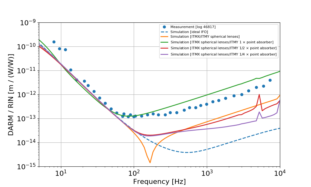
- with the "improved" locking, the simulation gets quite close to the measured RIN coupling
In the figure below, the coupling from RIN to DARM is shown for three configurations
- ideal IFO, all perfectly matched, no lenses, no mismatch
- spherical lenses: both ITMX and ITMY substrates contain a spherical lens with focal given by Aidan's numbers (ITMY self heating is modeled with an uniform absorption of 0.36 ppm)
- sperical lens in ITMX, measured point absorber map in ITMY (full amplitude of the optical path distortion, 1/2 of the amplitude and 1/4 of the amplitude for reference)