jeffrey.kissel@LIGO.ORG - posted 11:00, Monday 18 April 2022 (62653)
Details of In-loop Front-end Only, Sub-Nyquist, OMC DCPD Electronics Response Compensation
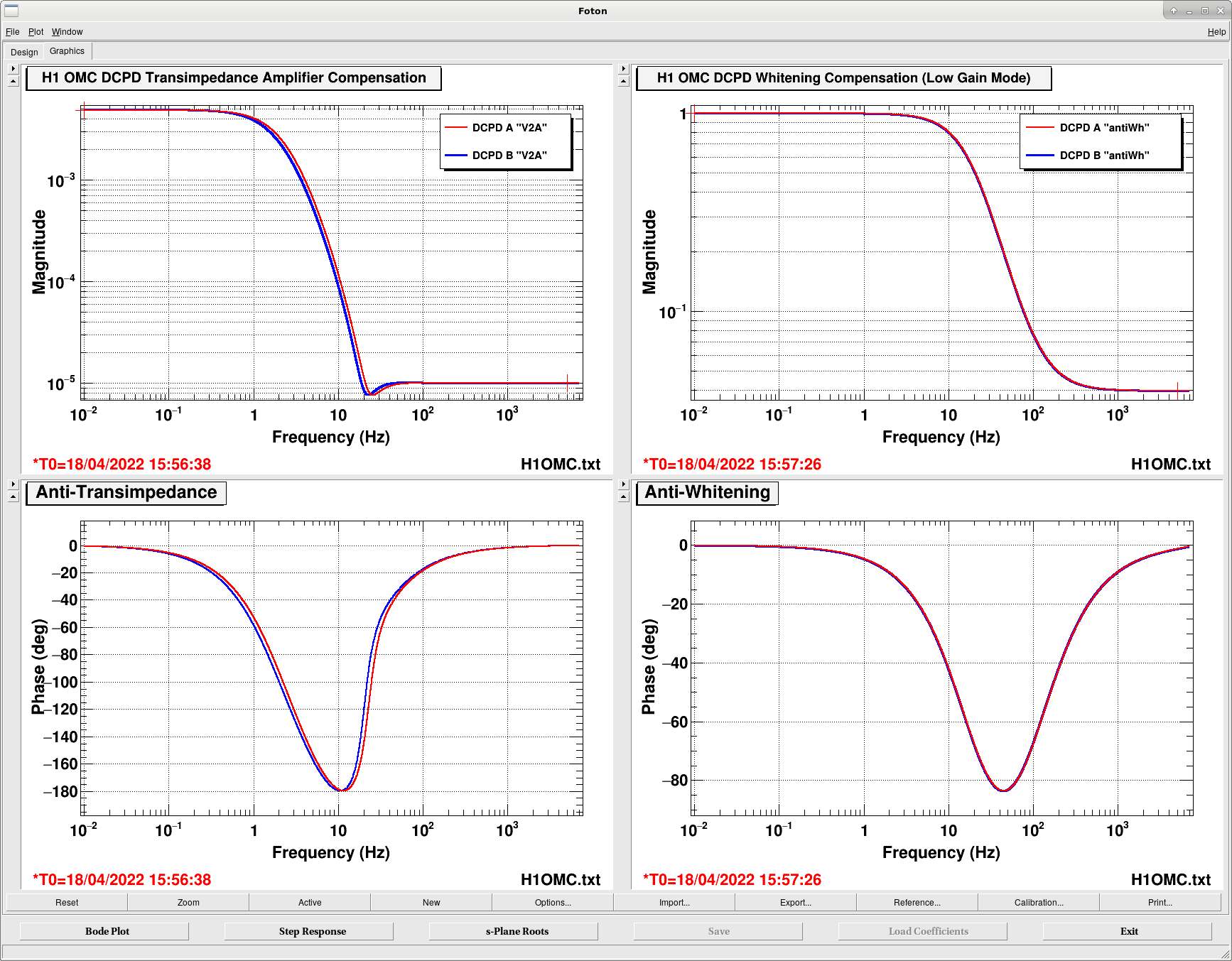
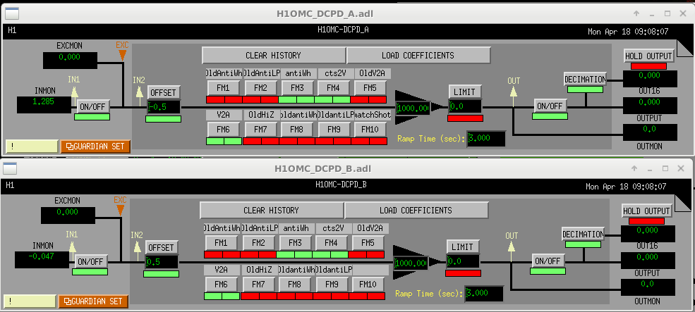
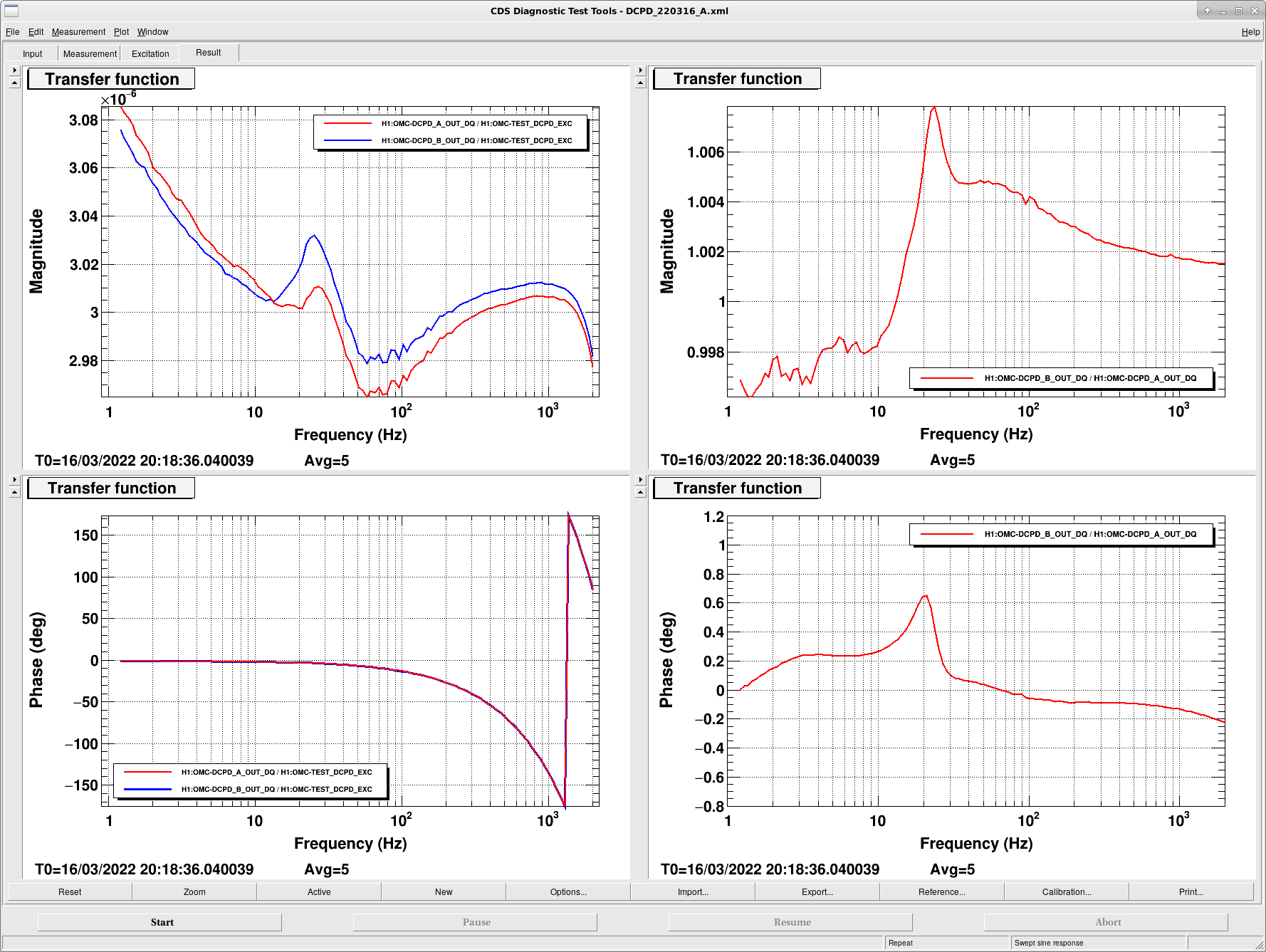
J. Kissel [for D. Sigg]

Back on March 15 2022 (LHO:62250) Daniel installed a compensation scheme for the new OMC DCPD (the GW DCPDs) A+ transimpedance amplifier (TIA) and whitening based on Dripta's fits of the data we took on Feb 15 2022 (LHO:61823 and LHO:62187). Then, he verified the installed compensation with a quick measurement using the newly available remote excitation system. This aLOG covers all the details implicit in that work.

%%% Installation Details %%%

Explicitly calling out what's installed,
    OMC_DCPD_A     FM6     "V2A"     zpk([5.699+i*22.223;5.699-i*22.223;32.73],[2.549;2.117;6.555],0.00501187,"n")gain(0.971763)
                   FM3     "antiWh"  zpk([91.44;111.63],[18.1;22.3],1,"n")
                   FM4     "cts2V"   gain(0.0006105)
                   GAIN    (A to mA) 1000.0

    OMC_DCPD_B     FM6     "V2A"     zpk([4.747+i*19.789;4.747-i*19.789;32.50],[2.533;1.667;6.477],0.00501187,"n")gain(0.98196)
                   FM3     "antiWh"  zpk([90.49;108.86],[17.9;21.8],1,"n")
                   FM4     "cts2V    gain(0.0006105)
                   GAIN    (A to mA) 1000.0
The plots of the individual filters FM6 and FM3 are shown in 20220418_H1_DCPDElectronics_OMCA_Compensation_FilterResponse.png, and screenshots of the MEDM screen locations of these filters are in 20220418_H1_DCPDElectronics_OMCA_Compensation_FilterBanks.png.

Verifying the numerical values of the zeros and poles of Dripta's fits, and conceptually against the components of the circuits (as reviewed in G2200551), there are a couple of compensation design decisions he made here that are worth mentioning:

    (1) For the TIA, he's chosen to normalize the compensation filter to have a gain of (exactly) 1e-5 [A/V] at the high frequency asymptote of both filters. This matches inverse of the *circuit schematic* value of the overall [A] to [V] conversion of the "GW path," of [V_DIFF / I_GW] 100e3 [V/A] where within the circuit (D2000592 -v3), that comes from
        - feedback resistive component R5 = 10e3 [V/A]
        - in-GW frequency band (between ~50 Hz and 5000 Hz) whitening gain (in [V/V]) of ~5 defined by the zero:pole pair at [~6.5:~32] Hz created by the input and feedback RC networks surrounding the U4 op-amp, and
        - the single-ended to differential ADC driver gain of 2.0 [V_DIFF / V_SE]

    (2) For the whitening filter, he's chosen to invert the low gain mode, which has a in-GW frequency band whitening gain of ~25 from the following components within the circuit (reading from D2100630 -v3)
        - one stage of whitening, with a zero:pole pair at [~20:!100] Hz from the RC networks surrounding U17 for a in-GW-frequency-band gain of ~5
        - another stage of whitening, with another zero:pole pair at [~20:!100] Hz from the RC networks surrounding U18 for another in-GW-frequency-band gain of ~5
    However, implicit in this choice, he's normalized the filter to have unit gain at DC, and lets the high-frequency gain fall where it may based on the exact zero:pole combination.
    (3) There are the ideal-exact-values for the (inverse of the) ADC gain, 1 / 0.0006105 = 1638.001638 [ct/V_DIFF]***, as well as the ideal conversation from [A] to [mA] "gain" (or unit conversion) of 1000.0. These items haven't changed, and are left from what was there before.
    *** This value is not the ideal exact value for the ADC. It should be 2^16 / 40 [ct/V_DIFF] = 1638.4 [ct/V_DIFF]. Why this is not exact, I don't know. If it were a measured value, I would expect them to be different between the DCPD A and DPDC B channels, but they're not.

The front-end cannot compensate for the 5 poles at ~10 kHz (two from the in-vac analog TIA, and three from the analog whitening chassis), so this will need to be compensated for in the low-latency GDS pipeline (and we'll also need to add a ~2.5e-6 delay to approximate phase loss from the 180 kHz feature caused by the SQZ path pick-off of the DCPD current in the TIA, and the 160 kHz feature caused by the last inverting op-amp stage in the whitening filter).

The .pdf attachment (20220215_H1_OMCA_DCPDTIA_S2100832_SN02_OMCA_DCPDWhitening_S2101608_etaR.pdf) shows the performance of this compensation scheme in terms of how the residual uncompensated response impacts the DARM loop response function (assuming no gain imbalance is left in the chain). One can see much more detail on how this is derived in G2200551, but in short:
    - We (obviously) need to compensate for the super-Nyquist, 10 kHz poles in the TIA and Whitening Chassis (compare "Rdx" traces which only have sub-Nyquist front-end compensation, against "Full" traces which have all the super-Nyquist poles and zeros from the fit). We will do so, as we've always done, in the GDS pipeline. But, it's instructive to show how bad the error is in R for front-end-only calibration.
    - Once we compensate for everything we measured / fit (the "Full" traces), there's still a residual ~1 deg phase loss at 1 kHz that increases to 4 [deg] by 5 [kHz]. This is a real phase loss attributed to *measured* impact of 180 and 160 [kHz] features in the TIA and Whitening Chassis respectively, but we don't have a fit pole frequency for them because they're above the measurement band of the SR785. So, we'll approximate the response with a 2.5e-6 [sec] delay in GDS.

%%% Verification of compensation via remote transfer function %%%

After installing this compensation, he used the newly built-in remote characterization system (see LHO:62235, LHO:62250, slides 71 through 76 of G2200551) to measure the product of (1) the analog TIA, (2) the analog whitening chassis (3) the digital compensation for the TIA, and (4) the digital compensation for the whitening, and got the results shown in 20220418_H1_DCPDElectronics_OMCA_Compensation_CharacterizationResults.png (shown in linear magnitude rather than in [dB], so we can read off the frequency dependence in percent and make an attempt to understand the units rather than hiding them in "dB").

This measurement is actually quite a bit more complicated to understand than the isolated analog electronics measurements of the TIA (LHO:61810)and the whitening chassis (LHO:62181), because it includes:
    [ ] The digital AI filter which converts the digital drive from 16 kHz to 65 kHz (from the OMC user model rate to the LSC IOP model rate), which has (almost) unity gain and phase-loss inducing notch filter,
    [-] The 16-bit DAC gain for the digital drive excitation,
    [ ] The analog AI filter which has (almost) unity gain and phase-loss inducing notch filter,
    [ ] The (almost) unity gain of the signal chain from the AI filter out to the test inputs on the in-vacuum TIA,
    [ ] The unity gain op-amp buffer that converts the test input voltage from differential to single-ended,
    [-] The 100e3 [V/A] series resistance that converts the single-ended test voltage into a current source,
    [-] The TIA amplifier response, which includes two uncompensated ~10 kHz poles
    [-] The whitening chassis response, which includes three uncompensated ~10 kHz poles
    [ ] The analog AA filter which has (almost) unity gain and phase-loss inducing notch filter,
    [-] The 16-bit ADC gain of the analog voltage coming in from the analog AA,
    [ ] The digital AA filter which converts the digital drive from 65 kHz to 16 kHz (from the LSC IOP model rate to the OMC user model rate), which has (almost) unity gain and phase-loss inducing notch filter, and finally
    [-] All the above mentioned digital compensation
where the bullets that are empty "[ ]" do not significantly impact the DC or in-GW band gain of the measurement, but have some non-negligible phase loss, and those that are full "[-]" do.

Thus, the transfer function should have a [mA / DAC ct] gain of something like
    [ ] ~1                       [OMC DAC ct / IOP DAC ct]
    [-] 20 / 2^16 = 3.052e-4     [DAC V_DIFF / DAC ct]
    [ ] ~1                       [AI V_DIFF / DAC V_DIFF]
    [ ] ~1                       [TEST V_SE / AI V_DIFF]
    [-] (1 / ~100e3)             [TIA A / V_SE]
    [-] The TIA response         [TIA V_DIFF / TIA A],     ~100e3 [V/A] at ~1 kHz
    [-] The Whitening response   [WH V_DIFF / TIA V_DIFF], ~25    [V/V] at ~1 kHz
    [ ] ~1                       [AA V_DIFF / WH V_DIFF]
    [-] 2^16 / 40 = 1638.4       [IOP ADC ct / AA V_DIFF]
    [ ] ~1                       [OMC ADC ct / IOP ADC ct]
    [-] (all at ~1 kHz):
        1000                     [mA / A]
        * 1.0e-5                 [TIA A / TIA V_DIFF]
        * ~1/25                  [TIA V_DIFF / WH V_DIFF]
        * ~40/2^16               [AA V_DIFF / ADC ct]
    = (20 / 2^16) * (1 / 100e3) * (100e3) * (25) * (2^16 / 40) * (40 / 2^16) (1/25) * (1 / 100e3) * 1000
    = (20 / 40) * (40 / 2^16) * (1 / 100e3) * 1000
    = ~3.051e-6 [mA / DAC ct] at 1 kHz

which is consistent with the magnitude of Daniel's results for each transfer function.
Also, delightfully, it appears as though the gain ratio of the two paths, is only deviates from unity by at worst ~0.5% right around the complex pole pair formed by the TIA.
Because of all the unaccounted for, high-frequency, phase loss (five 10 kHz poles, plus four AI / AA filters), the transfer function loses 180 [deg] of phase already by ~1 kHz, but no surprise there. In the future, we can export this data, and pull out all of those known features.

So, while there's a lot more to consider, Daniel's results at least make sense, they report / confirm that the compensation is excellent when he measured it on 2022-03-15, and will be useful as a quick diagnostic looking for any change over time, like has been experienced at LLO LLO:59540.
Images attached to this report
Non-image files attached to this report
