This morning we sat in nominal low noise without going to observing from 19:21 to 19:51 UTC (Jan 9th) in a configuration that should be much better for the 1084Hz glitches. (WP6420)
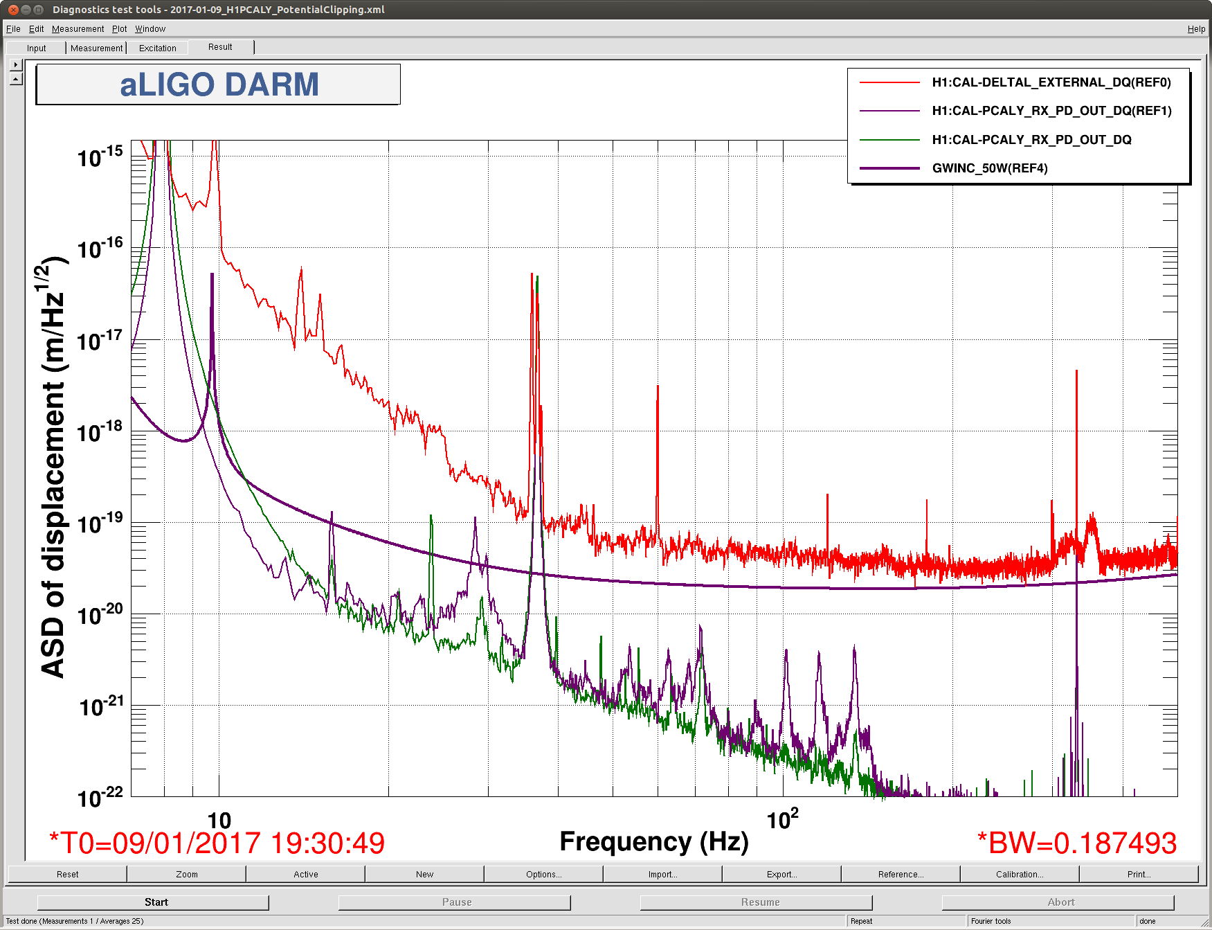
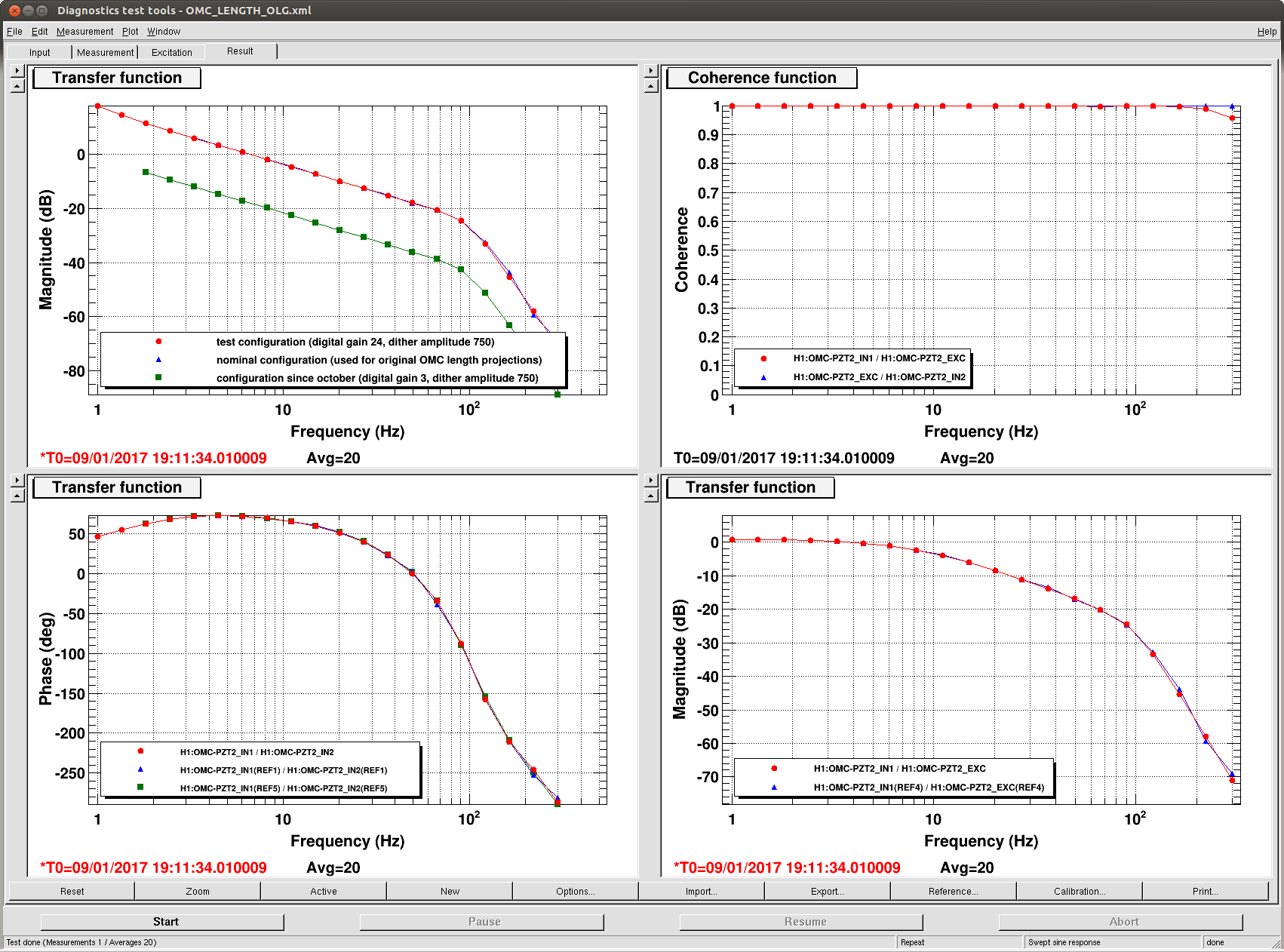
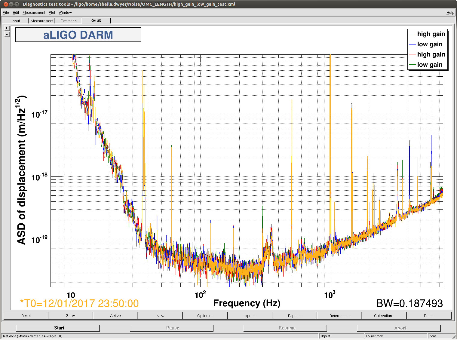
On Friday we noticed that the 1084Hz feature is due to OMC length fluctuations, and that the glitch problem started on Oct 11th when the dither line amplitude was decreased (alog 30380 ). This morning I noticed that the digital gain change described in alog 30380 that was intended to compensate for the reduced dither amplitude didn't make it into any guardian, so that we have had a UGF that was a factor of 8 lower than what I used when projecting OMC length noise to DARM: 30510 The first attachment shows open loop gain measurements from the 3 configurations: before oct 11th (high dither amplitude), after october 11th (lower dither amplitude, uncompensated) and the test configuration (lower dither amplitude, compensated).
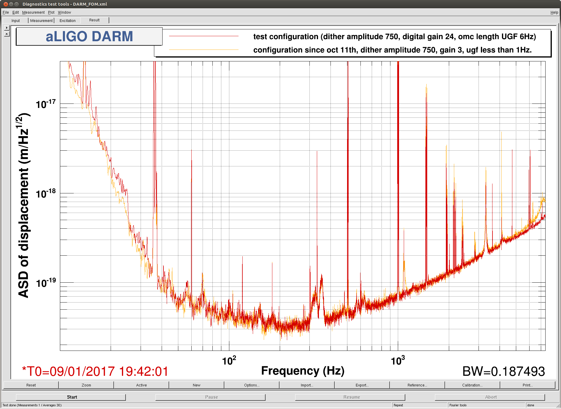
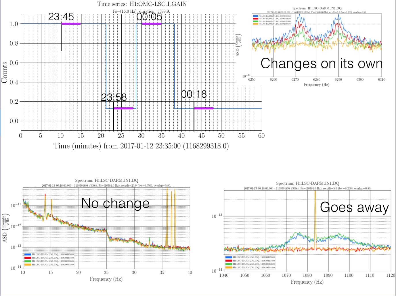
We ran with the servo gain set to 24 (to give us the nominal 6Hz ugf) and the lowered dither line amplitude from 19:21 UTC to 19:51 UTC Jan 9th. You can see the spectrum durring this stretch in the second attached screenshot, in the test configuration the peak around 1083Hz is gone, with just the pcal line visible, and the OMC length dither at 4100Hz is reduced by more than an order of magnitude. You can also compare the glitches from this lock stretch with one from yesterday to see that the glitches at 1084 Hz seem to be gone. This is probably the configuration we would like to run with for now, but we may try one more test with increased dither line amplitude.
Other notes because we don't have an operator today due to weather:
This morning all 4 test mass ISIs were tripped probably from the Earthquake last night that brought the EQ BLRMS to 10 um/second around midnight UTC. ITMY tripped again while it was re-isolating, no problem on the second try.
Richard topped added 400mL to the TCSY chiller around 10:15 or 10:30 local time, since we were getting low flow alarms. The flow alarms came back a few minutes before 11am local time.
I went through inital alingment witout problems and got to DC_readout transition. Then I measured the UGF of the OMC length loop in preparation for increasing the dither line height From that measurement and trends it became clear that when the OMC dither amplitude was reduced, the compensation of the OMC digital gain described in didn't make it into the guardian. This means we have been operating with a UGF in the OMC length loop that was a factor of 8 too low since mid october.
We arrived in low noise at 19:21 UTC with the OMC ugf increased to 6Hz. After about a half hour PI modes 27 and 28 rang up, and I wasn't fast enough to get them under control so we lost lock.

Took ISI CONFIG to BIG_EARTHQUAKE_NOBRSXY after the lockloss & stayed there for about 30min (6:40-7:12utc) per text from Warner.
Now just holding at LOCKING_ARMS_GREEN until noticeable seismic motion (seen via ALSx/y & Tidal traces) decays, also per text from Warner (who is inbound shortly).
Seismic band (0.03-0.1Hz) has dropped down to 0.5um/s now.