I have spent some time trying to understand the behavior of the CARM loop in full lock.
First, I have reduced the loop to the following block diagram:
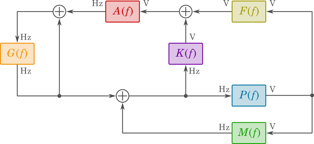
P is the IFO, K is the IMC, and G is the FSS. F and M represent the fast and slow common-mode feedback paths, and A represents the IMC PDH board and the VCO. A fuller accounting of these blocks is given in the sections below.
The OLTF of CARM is then given by
where is the CLTF of the FSS. For the time being, I have ignored the slow IMC feedback (the crossover with the fast path happens below 100 Hz) and I have assumed the CLTF of the FSS is −1.
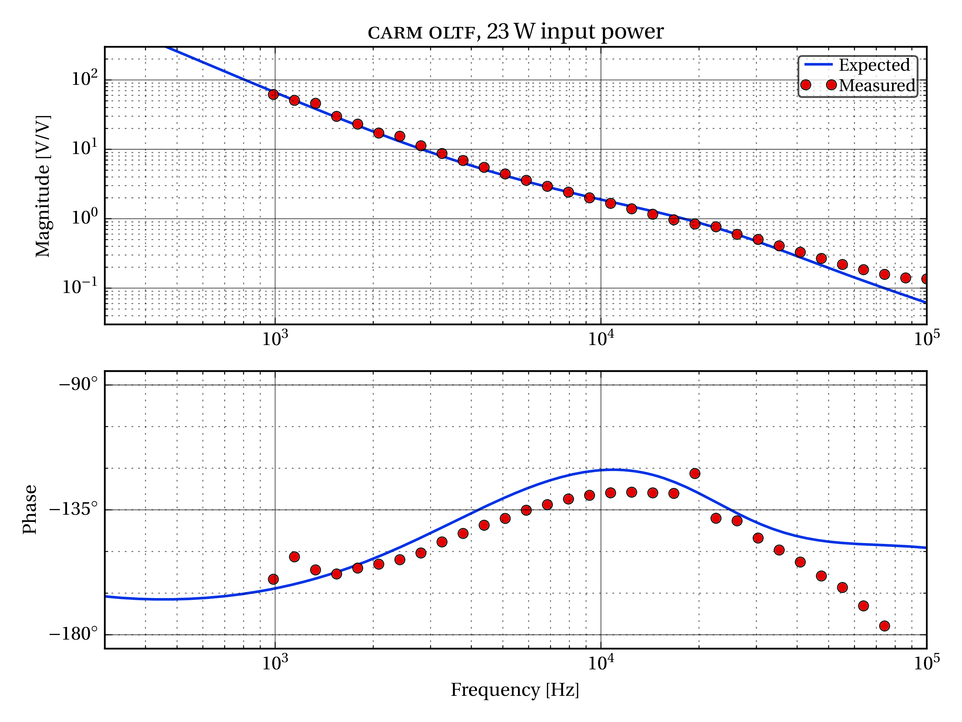
The model (described below) shows OK agreement with the measurement (taken 2015-08-14) between 1 and 40 kHz, but above that there is significant deviation in the phase.
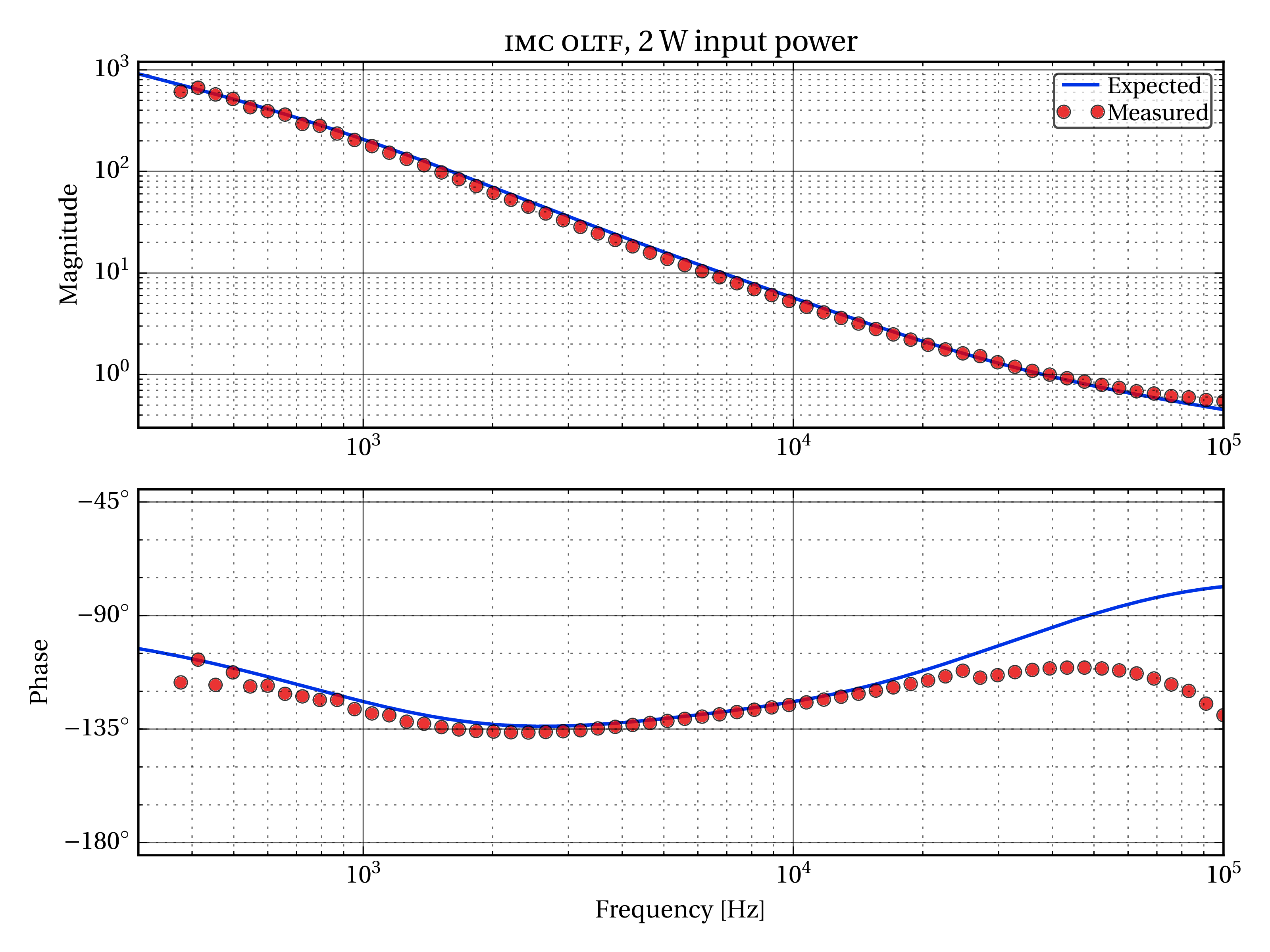
I have also included a plot of the modeled IMC OLTF . Getting the model to agree with the measurement requires the inclusion of a mystery gain of 1/3, which I have rolled into the optical plant. Previous measurement of the IMC modulation index provided only an upper limit (which I have used here), so I am hoping that this explains some of the mystery gain.
❦ P(f): CARM optical plant, PD response, and CMB common path
The CARM plant is the TF taking laser frequency fluctuation to rf power on REFL9Q. It consists of the following (at 24 W):
- dc gain 0.017 W/Hz [from Kiwamu's numerical/analytical analysis, assuming 300 mW of light on REFL9 out of lock and a 9 MHz modulation depth of 0.22 rad]
- pole at 0.48 Hz [from Kiwamu's numerical/analytical analysis]
- pole at 8.8 kHz [from transmission through the IMC]
This is multiplied by the PD TF, the SNB TF, and the CMB common TF:
- dc gain of 2900 V/W from REFL9Q + demod
- dc gain of 0 dB through the SNB
- dc gain of −20 dB (CMB input gain)
- 40 Hz pole, 4 kHz zero, ac gain of 1 (the CMB compensator)
Note that since this measurement we've added 7 dB to the common gain, and correspondingly removed 7 dB from the fast and slow paths. But that shouldn't matter for the OLTF estimate.
❦ F(f): CMB fast path, IMC ao gain
- dc gain of 7 dB (CMB fast gain)
- two zeros at 0 Hz, two poles at 5 Hz, ac gain of 1 (CMB fast HPF)
- dc gain of −2 dB (IMC ao gain)
❦ M(f): CMB slow path, MC2 suspension
Not yet implemented. So far I have only considered the portion of the loop for which |AF| ≫ |M|.
❦ K(f): IMC optical plant, PD response, IMC board input gain
IMC optical plant, 24 W:
- dc gain of 4.1×10⁻⁷ W/Hz [46 mW on IMC REFL out of lock (LHO#20117), modulation index 0.04 rad (upper limit; LHO#9395), fudge factor of 0.35]
- pole at 8.8 kHz
PD response 880 V/W [responsivity 0.37 A/W (LHO#5277), transimpedance 476 V/A (ibid.), demod TF 5 V/V (rf volts to if volts; D0902745)]
IMC REFL input gain −3 dB [nominally 17 dB at 2.5 W PSL power]
❦ G(f): FSS OLTF
Currently, the CLTF G/(1 − G) is assumed to be −1. I have a measurement of G from Peter K, but I have not yet included it here. Below 100 kHz, the CLTF deviates from −1 Hz/Hz by less than 50 % in magnitude and 5° in phase (see attachment).
❦ A(f): IMC common/fast path and IMC VCO
IMC common/fast path TF:
- 40 Hz pole / 4 kHz zero, ac gain 1
- 1 kHz pole / 20 kHz zero, ac gain 1
- dc gain −6 dB (IMC fast gain)
- 140 kHz pole / 70 kHz zero, dc gain 1 (IMC fast path HPF)
IMC VCO TF:
- dc gain: 537 kHz/V (installed in SFM for the IMC VCO)
- pole at 1.6 Hz, zero at 40 Hz

Evan has told me that the above diagram and OLTF equation are wrong.

He's given me the liberty to preempt the publication of his thesis and provide the erratum for this entry.

The open loop gain transfer function of the CARM loop is defined by the attached diagram,

H = bar{G} A K P (F/K + M) / (1 - bar{G} A K)

Where again,
G = open loop gain of the FSS
bar{G} = G / (1-G) = closed loop gain TF of the FSS
A = the IMC Common Mode Board and IMC VCO
P = electro-optical CARM plant of the IFO
K = electro-optical IMC plant
F = CARM fast path through CARM Common Mode Board (fed to the input of the IMC Common Mode Board to IMC VCO)
M = CARM slow path to IMC Length control of MC2