jeffrey.kissel@LIGO.ORG - posted 15:52, Monday 21 February 2022 - last comment - 22:35, Thursday 10 March 2022(61810)
Measuring the New OMC DCPD Transimpedance Amplifiers in Detail; A Learning Experience
D. Bhattacharjee, J. Kissel

[1] Actual Board S/N SN 02
[2] In-vac "QPD" Enclosure S/N S2100832
[3] Transimpedance Circuit Schematic D2000592
[4] Transimpedance Design Document T2000698
[5] Benchtop Measurement and Fitting Results T2100403
[6] Whitening Chassis interface D2100630 (Whitening Chassis S/N S2101608)
[7] OMC Wiring Chain D2100716

Last week, we attempted (and eventually succeeded in) a repeat, careful version of the measurements of the new OMC DCPD Transimpedance Amplifiers (TIAs) described in LHO aLOG 61515. The measurement setup (in diagram, picture, and text of SR785 settings form) and quickly-plotted results are attached, accompanied with menagerie of bad data we took in order to get there. Quite a learning experience, with this new transimpedance amplifier [3] and even newer OMC whitening chassis [6] we used to characterize it.

We've now got good data, and fitting / modeling / compensation aLOGs are to come, but the experience to get that good data is worth it's own aLOG. This is that aLOG.

%%%%
Lessons Learned:
(!) (The royal) we really wish (the royal) we would have measured the test input's series resistors (R1; nominally 100 kOhm) before enclosing the TIA circuit in it's QPD enclosure and closing HAM6. Water under the bridge now, but because we didn't, we can't precisely / accurately divide it out the measured series resistance of the test input to get the units ([V/A]) and precision DC calibration for the actual PD's path circuit that we really want.
(@) The OMC whitening chassis's "From DAC" Test (signal) Input connector J7 (and J7 only) does not conform to LIGO standards (T060123) for which pins to use for the positive and negative legs of a differential signal chain.
(#) The benchtop data set [5] for these TIAs has a minus-sign in it due to the quirks of *it's* measurement setup.
($) Something fishy is going on with the power & test relay such that occasionally, the gain of the OMC A DCPD B path would be half (1.0/2.0) what's expected, and could be resolved by toggling the switches a few times (and spinning around twice, on one foot, while touching one's right ear with your *left* thumb).
(%) We *must* turn off the Auto Offset feature of the SR785s response channels during these long ~20 minute measurements.
(^) We *must* make sure that all breakout boards are thoroughly engaged to the "connectors under test" in order to get a reliable DC Gain measurement.
(&) The DB9 breakout board in my measurement setup had no clean, secure way to connected the shields of the differential BNC connection from the SR785 Accessory Box to the electrical ground / 0V of the whitening chassis Test Input. It will remain unclear if that poor connection influenced the gain or frequency response of the measurement.

So. Let's talk about Bruno.

%%%%
Attachment 1: D1900027-v3_aPLUSO4_D2100630-v2_OMCDCPDTransImpAmp.pdf
    This is a revised set of diagrams from those shown in LHO:61515 that conveys the characterization measurement setup, both with the transimpedance amplifier engaged in the measurement setup (page 1), and with the transimpedance amplifiers bypassed and such that only the measurement system is characterized (page 2).

    The improvements includes
    (a) an accurate reflection of where the positive and negative legs connect for the test input, now that I understand Lesson (@) from the above list is the truth, rather than just a typo in the drawing, and
    (b) a second page that shows how to extract the test input from the front of the chassis as it goes out to the in-chamber DPCD TIAs as the response for the "measurement setup" transfer function.

%%%%
Attachment 2: 2022-02-15_OMCDCPDTIA_WhiteningChassis_MeasSetup.pdf
Here's a collection of pictures, with labels, instruction, and words of caution.
    Page 1: The Test Input "To DAC" spigot at the back of the chassis.
    Page 2: The "DCPD A" DB25 spigot, which is actually for *OMC* A's DCPD A and B (hence the overriding sticker label above the spigot), out of which the Test A excitation goes to the chamber, and the DCPD TIA response comes back from the chamber.
    Page 3: Similar picture as page 2, but showing the setup configuration while testing DCPD B's TIA.

%%%%
Attachment 3: 2022-02-15_OMCDCPD_WhiteningChassis_MeasurementNotes.txt
    These are the notes of the SR785 setup we took during the measurement.

Of critical note within these settings notes is
    - the SR785's output SRC voltage amplitude of 4 [V_pk, single-ended], which feeds to the SR785 accessory box, which converts that to 2 [V_pk, on each leg], or 4 [V_pk, differential]. I picked that amplitude, because I assumed that this test input was designed to handle the drive from a standard LIGO DAC, which has range 20 [V_pkpk, differential], or 10 [V_pk, differential], or 5 [V_pk, on each leg], i.e. 20% less than my assumed full range of the intended drive system. With this amplitude, the "Test+" and "Test-" of the TIA circuit [3] each receive 2 [V_pk, on each leg], which is converted to single-ended "TestSig" via the U13 AD620 op-amp, which is connected in parallel via relay to the "Photodiode1 Pin 1" the DCPD A anode (+) or to the "Photodiode2 Pin 1" DCPD B anode (+). This is also not terribly different from the test amplitude of 1 [V_rms, one leg] = 1.414 [V_pk, one leg] that was used during bench-top testing (see Table at the top of page 4 of [5]).

    - In the input menu, the Auto-offset feature is turned OFF for both Channel 1 and Channel 2. See Lesson (%) above and (x) below

    - In these measurements, we overlooked the Settle Time / Settle Cycles parameters of the Swept Sine Average Menu, and set the Settle Time to ~11 [ms] and Settle cycles to 5. That meant that, with the Integration Cycle number at 5, i.e. 5 averages per frequency bin, the 0.1 Hz data points were sending in 5 + 5 cycles = 100 [sec] worth of data to get 1 point. With 200 logarithmically spaced points between 0.1 Hz and 102.4 kHz, you spent 22.5 minutes gathering the data from 0.1 Hz to 1 Hz, and averaging doesn't switch to "Integration Time" until ~900 Hz. Since this is an electrical system, with a relatively low Q resonance, we could probably easily get away with reducing the Settle Cycles from 5 to 2, even while increasing increasing the Settle time to 152 [ms] to match the integration time to decrease the cross-over frequency between time and cycles from 60 to 20 Hz, and still reduce the total measurement time from 25 minutes to 17 minutes. This is to-be-determined by the fitting process, but we could even increase the lower frequency bound of the measurement from 0.1 Hz to 0.2 Hz, and (with the same averaging parameter adjustments) reduce the measurement time to 10 minutes. I made all these compromises (albeit not so consciously, nor back with math) in January 2022 with the PUM drivers, and it worked out just fine. However, for this brand-new circuit, with less channels to measure, and the low-frequency ~1 Hz zeros, and a desire to *actually* gather the "DC" gain, I went with 0.1 Hz. Ah well. We shall consider again next time we measure and after we're done fitting. It's easy to strip *out* data in post-processing with fits in hand to test out these hypothesis, but very challenging to convince someone with modeled extra data you didn't gather.

    - Also considering total time of measurement, I chose 5 V/sec ramp on the source as well rather than the typical 1 V/sec. On a SR785, the settle-cycle count doesn't start until the source amplitude is fully ramped up, so I wanted to keep a ramp on, but get to the cycle counting as soon as reasonably possible (ASARP). With my drive amplitude of 5 [V_pk], that means the source was ramped on fully only after a second, and with my frequency vector configured to sweep *up* rather than *down* (because fStart is lower frequency than fStop in the frequency vector menu), then it got to the counting the 0.1 Hz settle cycles ASARP.

In some glorious amazing future when
   - not every measurement is an explorative measurement,
   - electronics designs are stable,
   - we don't need the answer completely measured / fit / modeled / compensated in less than a week all by one person, and
   - the GPIB + CDS WiFi system is well-maintained,
we should spend the time to write a GPIB script for these parameters and to automatically extract the answer, rather than having to remember to review the details while you're sitting on the floor managing 60 other critical details. But for now, a human "wasting" a little more time next to the racks, is good enough.

%%%%
Attachment 4: 2022-02-15_OMCDCPDTIA_OMCA_DCPD_RawMeasurementResults.pdf
A collection of 3 .pdf plots showing various results.
    Page 1: This shows our "final answer" data set that we'll be using for zero:pole fitting. This is much like the data from LHO:61515, but the data extends down to 0.1 Hz in order to obtain good resolution -- and thus good fits -- of the expected zeros around 1 Hz.
       - Using the same, "who knows how accurate?", R1 series resistance of 100 kOhm, the DC transimpedance of the TIA is 2.5e-8 [V/A], and the DCPDA and DCPDB channels differ by only 1%.
       - The transimpedance at ~200 Hz is 10e-6 [V/A].
       - Even without compensation, the transfer function ratio above ~200 Hz has magnitude matched better than DCPDA/DCPDB = +/-0.2%, and phase match better than 0.2 [deg]

    Page 2: This shows the results from the "measurement setup" transfer function (page 2 of attachment 1) -- both with the BNC clip leads of differential drive from the SR785 accessory box connected (i) as designed (albeit incorrectly) with Pin 6 of the DB9 as the positive leg, and Pin 1 as the negative leg; the "Good" data and (ii) vice versa, with Pin 1 as the positive leg, and Pin 6 as as the negative leg; the "Bad" data. While if might be obvious to anyone and everyone, it was when I was gathering (ii) that the lightbulb first went off that the phase of the TIA's transfer function should be asymptote-ing to ~0 [deg] at low frequency, not -180 [deg] as is shown in my original measurement (LHO:61515) and *is also shown in the benchtop testing data* [5]. So, I re-took the data with the clip-lead differential legs reversed, not only to triple-confirm that the whitening chassis [6] is wired differently from convention, but also because I was in "calibration" mode, so had to be super sure that one can account for reversing the polarity of the legs but "just" multiplying by -1.0. Turns out, yes, flipping the polarity on the legs *can* be modeled by a simple " -1.0 x " in the transfer function, with systematic error only at the 50 ppm / 0.4e-3 deg level (though the phase error does increase with frequency starting ~2 kHz to 3e-3 [deg] at 100 kHz.)

    For consistency and sanity's sake, I re-took the final dataset with the test inputs connected as designed, in the (i) configuration, as shown in the diagrams of Attachment 1. Regardless, this "measurement setup" transfer function is divided out of the data, such that *whatever*'s going on with it (namely, the ~0.994 DC gain, and the frequency dependent wiggles at the 0.2% / 0.2 [deg] level), we need not concern ourselves, nor confuse the fitting routine, with it.

    Page 3: This shows in a myriad of ways why we need to be so dang careful and explicit with every little detail in these measurements. I compare the final answer "good" result from DCPD A's transimpedance amplifier, against the several other measurements that suffered from us *not* remembering / paying attention to every single detail. The three bad conditions (each with the measurement setup divided out) are:
    (x) Auto-offset Mid-Measurement "AAMM": Forgetting to turn off the SR785's response channel auto-offset feature, such that several data points have statistically significant outliers in the magnitude and phase. Yes, it's only a data point or two, but in my experience, these kind of "glitches" confuse fitting routines. And since I haven't figured out or been made aware of how to extract transfer function coherence (or how to convert the equivalent uncertainty metric "normalized variance") from the SR785, I can't analytically / generically / routinely / algorithmically excise these data points without the pain of extracting them by hand (and remember that I'm having to do a *lot* of transfer function dividing in these processes, so if I excise points then I'd end up with different frequency vectors, and that opens a whole new can of interpolating, data fudging, etc.). I also note, retrospectively, that (y) and (z) setup flaws were also going on during this measurement, since this was one of the first measurement attempts of the day.
    (y) Test Input Breakout Board Loose "TIBBL": Not checking if the breakout boards are fully engaged into the chassis sockets. In this case, it was the Test Input DB9 that wasn't thoroughly engaged. An honest mistake during measurement setup that we only found after driving the DCPB path, and found that the gain of the transfer function was half of what we expected, i.e. Lessons ($) and (^). Even after engagement, ($), would still happen occasionally, so it wasn't the solution to that problem, but it was important to correct. Why? Because, apparently, there's a frequency-dependent, ~1.5% magnitude error that gets induced as is shown on the plot! Note, (z) setup flaw was present in this data set, since it was taken before the above mentioned light bulb went off.
    (z) Pos. & Neg. Test Input Legs Flipped "PNTILF": Having the positive and negative legs from SR785 accessory box incorrectly mapped to the Test Input DB9, i.e.  flipped, i.e. as discussed in (ii) above.

%%%%
Dripta will be posting the fitting and modeling results for this hunk of electronics.
Non-image files attached to this report


Comments related to this report
The data, and the quick plotting script used in the main aLOG above can be found committed to the CalSVN repo here,
    ${CalSVN}/Common/Electronics/H1/Data/OMCTransimpedanceAmplifier/S2100832_SN02/2022-02-15/
        # Raw "final good" data, in [PD TIA OUT V/ TEST CHASSIS REAR INPUT EXC V]
        # (both numerator and denominator are differential V volts)
        2022-02-15_OMCDCPDTIA_OMCA_DCPDA_mag.TXT
        2022-02-15_OMCDCPDTIA_OMCA_DCPDA_pha.TXT
        2022-02-15_OMCDCPDTIA_OMCA_DCPDB_mag.TXT
        2022-02-15_OMCDCPDTIA_OMCA_DCPDB_pha.TXT

        # Measurement setup, in the "good," + leg of Accessory Box going to + leg of the
        # Test Input [TEST CHASSIS FRONT OUTPUT V / TEST CHASSIS REAR INPUT EXC V ]
        # (both numerator and denominator are differential V volts)
        2022-02-15_OMCDCPDTIA_MeasSetup_mag.TXT    V]
        2022-02-15_OMCDCPDTIA_MeasSetup_pha.TXT

        quick_plot_data_20220215.m
The fitting script lives in : https://git.ligo.org/Calibration/ifo/-/tree/main/scripts/omctransimpedanceamplifier/fits

The fit results are as follows:

DCPDA
Fit Zeros: [2.549 2.117 6.555] Hz
Fit Poles: [1.108e+04 -0.j    3.273e+01 -0.j    1.022e+04 -0.j    5.699e+00-22.223j
 5.699e+00+22.223j] Hz
Fit Gain: 1135.512

DCPDB
Fit Zeros: [2.533 1.667 6.477] Hz
Fit Poles: [1.116e+04 -0.j    3.250e+01 -0.j    1.017e+04 -0.j    4.747e+00-19.789j
 4.747e+00+19.789j] Hz
Fit Gain: 1138.912

Both DCPDA and DCPDB has equal number if poles and zeroes, which is good. DCPD B has zeroes at lower frequencies than DCPDA. There is a complex pair of poles at 22.9 Hz for DCPDA and 20.3 Hz for DCPDB.  Also there are two poles at ~ 11KHz. These are what we expect from the transfer functions.
Non-image files attached to this comment
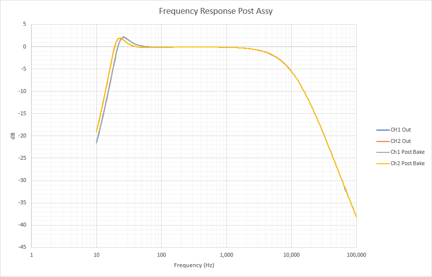
For the curious, there's been a side conversation about why the DCPD A and DCPD B response are so different.

See a zoomed out version of the ratio between A and B in final data in this attachment 2022-02-15_OMCDCPDTIA_OMCA_DCPD_FinalAnswer_zoomout.pdf.

The royal we (Rich Abbott, Dean Schaetzl, Daniel Sigg, Ali James, etc.) went back and looked at the data taken on the LHO unit before and after the bake, because someone guessed that might be why the component values are so different. Check out that data in PreBake_vs_PostBake_TIAAmplifier_SN02.png

The pre and post bake data are essentially identical at this zoom level. Said differently, the channel to channel differences seen at LHO are present in the "before" and "after" data seen prior to the shipment to CIT. Said differently again: th bake didn't change the capacitor values.

We also note that the LLO unit (S2100380, SN01) had much more variability than the LHO unit.

But -- saying it out loud for those who haven't heard -- it's not that this is any sort of show stopper. As you can see from Dripta's data above, we've measured the system carefully enough to get excellent fits for the future, and always planned, compensation of *any* / *all* of this response from each channel.

It just stinks that we can't just get "good enough" by "just" computing the 1/(2*pi*R/L) or 1/(2*pi*R*C) poles and zeros from the schematic values. We're looking in to how we can both getting more consistent parts, and measuring component values prior to in-vacuum sealing.
Images attached to this comment
Non-image files attached to this comment
I made a mistake in the script. Instead of multiplying the magnitude of the transfer function which we get in V/V with the series resistor, I divided by it yielding a A/V instead of correctly yielding  V/A.

The corrected script lives in: https://git.ligo.org/Calibration/ifo/-/tree/main/scripts/omctransimpedanceamplifier/fits


The updated plots are attached. Note the scale of the Y-axis changes because of the correction but the fit results remain unchanged.
Non-image files attached to this comment