Sheila, Georgia
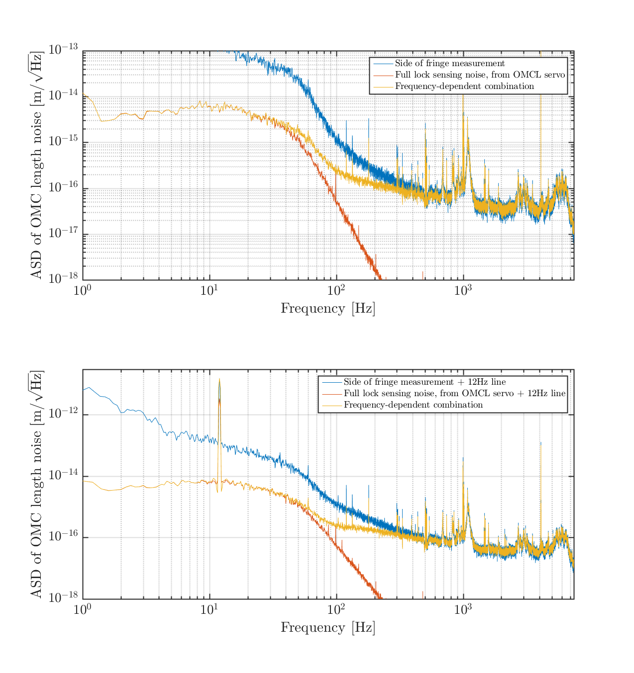
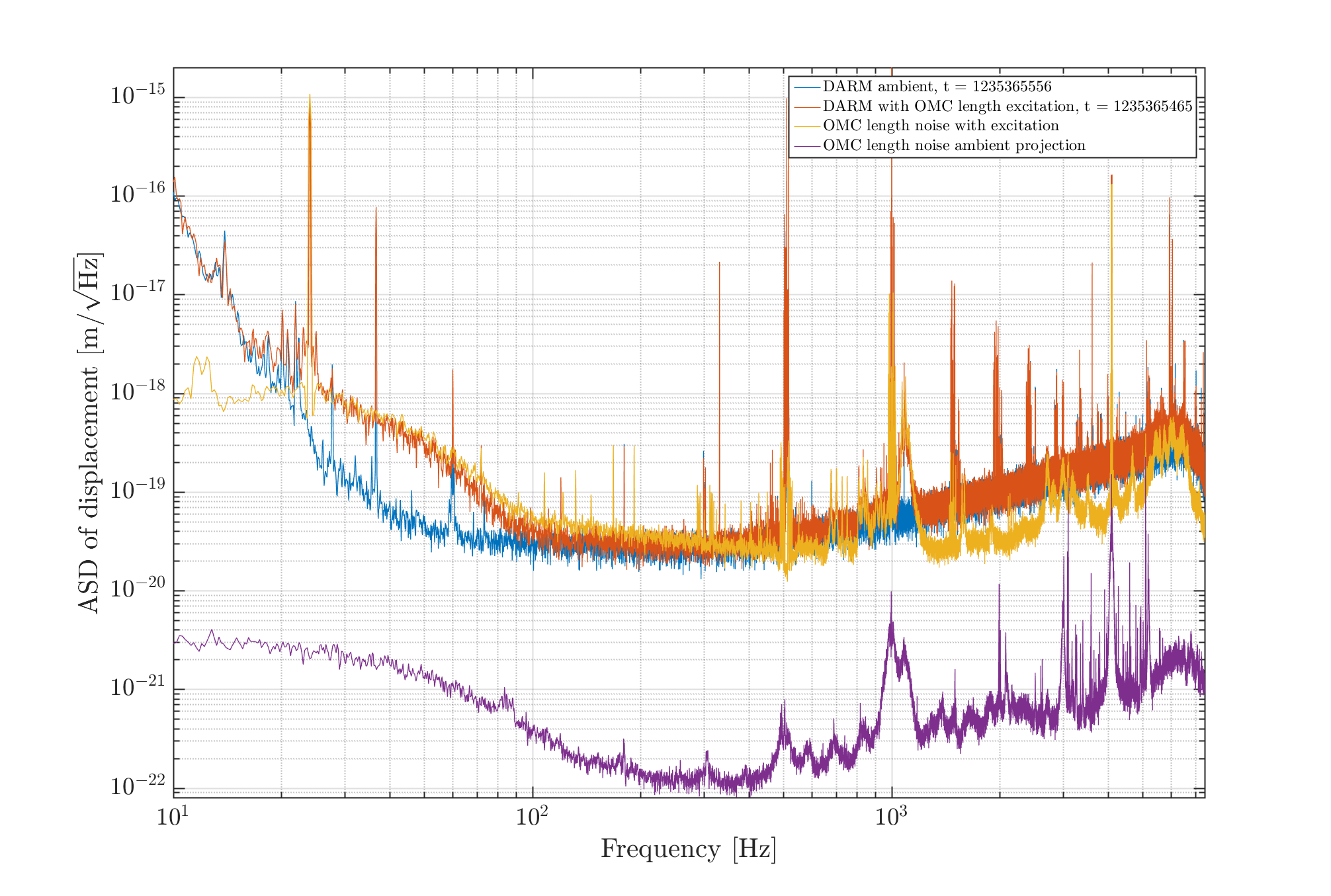
We have taken measurements of the OMC length noise - the top plot of the first attachment shows the length noise ASD in yellow - and projected it to be a factor of 30 below DARM at its closest point (second attachment). In the second attachment the blue and purple curves are DARM and the OMC length noise projection with no excitation. The red and yellow traces are taken when a 12 Hz line is injected at OMC PZT2, causing a 24 Hz line in DARM (OMC length to power on the DCPDs is a quadratic coupling), and additional broadband length noise below 100 Hz, and around the 1080 Hz resonance in HAM6. The prediction of length noise to DARM around 100Hz is a little off but this isn't unexpected given the way we have combined to witnesses of length noise, details below.
---
This measurement is a bit convoluted. When the OMC is on resonance the coupling from change of cavity length to power on the transmission DCPDs is quadratic (figure 1 in Dan Hoak's alog (19212) about exactly this measurement taken 2 years ago). To make a linear coupling from change in length to power on the DCPDs we can lock the OMC with an offset in the servo, i.e. on the side of a fringe. From the noise on the DCPDs while locked on the side of the fringe, and knowledge of how far off resonance we are, we can work out the change in OMC length this corresponds to. The maths for this conversion is summarised in the pdf attached to Sheila's alog (30510) about this measurement in 2016, and the script I used to make this projection is in:
/ligo/home/sheila.dwyer/Noise/OMC_LENGTH/2019/calibrate_DCPD_spectra_750_blend_servo.m
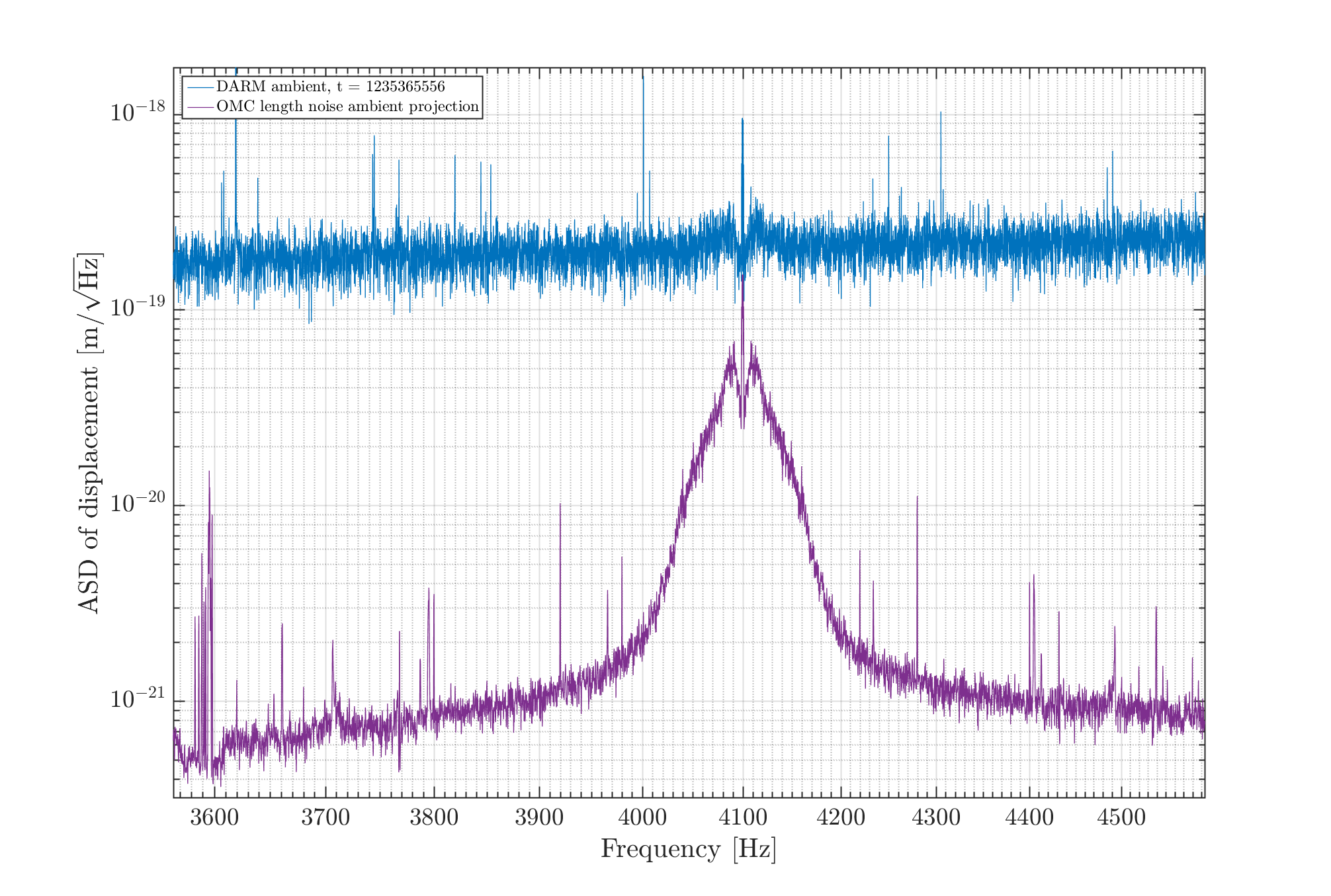
When we lock on the side of the fringe, above a few hundred Hz we see length noise. However around the dither line which the OMC length is locked to (4100 kHz), there is extra noise which then gets down-converted. This extra noise limits this measurement at low frequency (extra noise below a few hundred Hz in the blue trace in the first attachment). To see below this noise we can look instead at the in-loop error signal when in full lock, as Sheila did in the previous length noise measurement. The red trace of first attachment shows this error signal filtered by the closed loop gain of the OMC length loop. We also tried looking at the drive signal to the OMC PZT2, but this was too noisy. So the actual OMC length noise projection is made by combining the low frequency component of the in-loop error signal, and the high frequency component of the side-of-fringe measurement, shown in yellow in the first attachment. The top plot in the first attachment shows the length noise with no excitations to OMC length, and the bottom plot shows the length noise with a 12 Hz line injected, which we'll use later as a sanity check when projecting to DARM. The combination of length noise witnesses is a bit of a guess in the 50-300 Hz region, which is why I'm not surprised out projection doesn't line up perfectly with DARM in this region.
We next convert the length noise in m into the DCPD RIN (using equation 1 of the pdf attached to alog 30510). Multiplying this by the full lock DCPD current and adding the DARM calibration in m/mA (and the cavity pole and optical gain), we can convert this projection into meters of DARM displacement. This gives the yellow and purple traces in the second attachment.
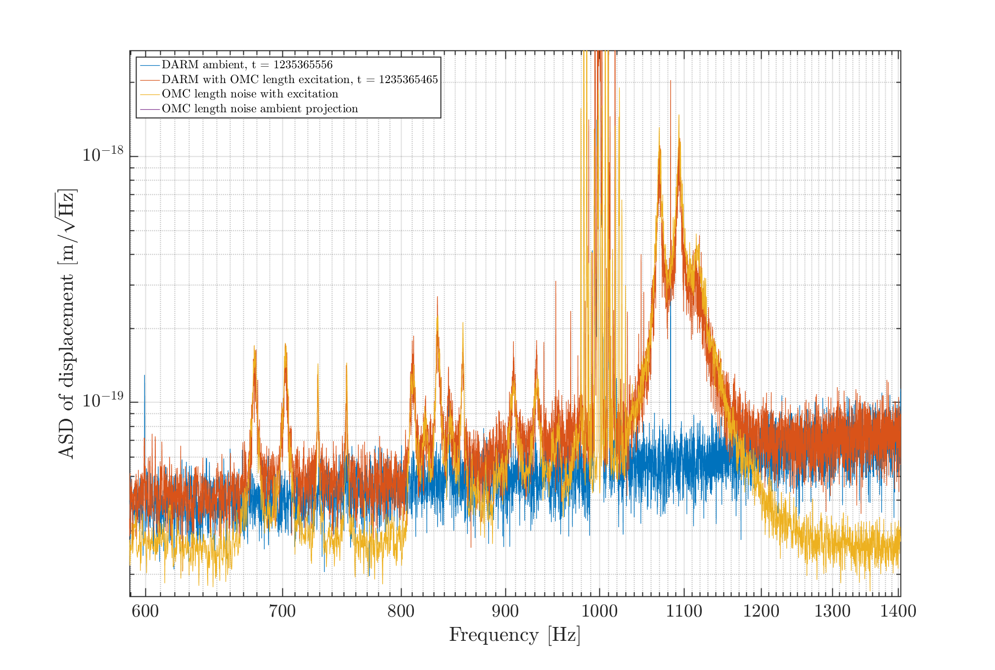
As a sanity check we inject a 12 Hz line into the OMC length (A=0.3, applied to PZT2) while locked on the side of fringe, and while in full lock. We can compare DARM and OMCL at the line frequency, the extra length noise around it, and the extra broadband noise around the 1083 Hz resonance (3rd attachment), it agrees well.
Some things to note:
Sheila, Nutsinee
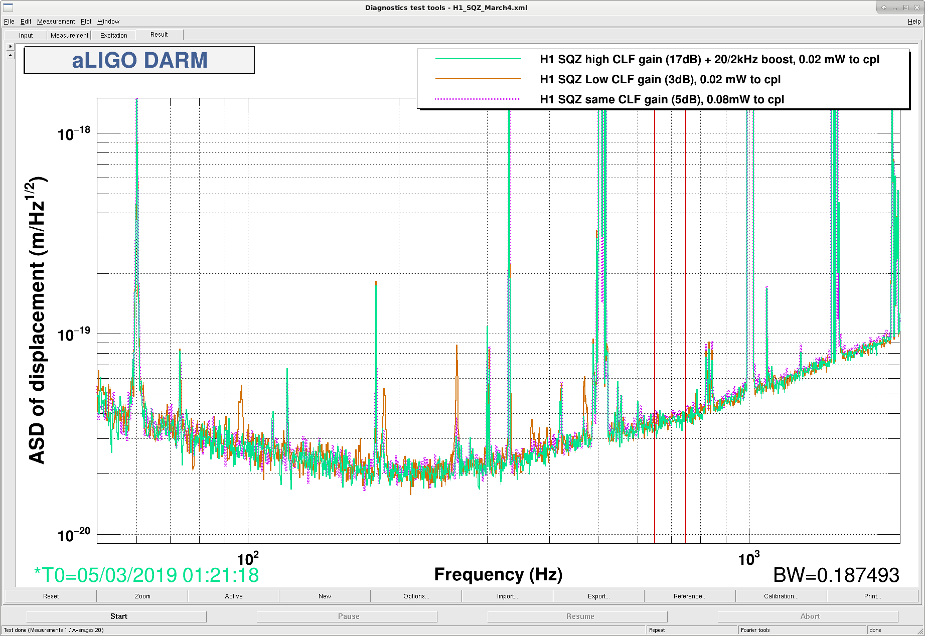
Following up alog47184 we investigated on how the other two peaks (one at 177.7Hz and the other at 262Hz) behave with different CLF power and UGF. The peaks only responded to decreasing/increasing loop gain but not to increasing power. We didn't do other tests (eg. noise eater on/off) since the IFO lost lock. We also tried decreasing LO loop gain but that didn't do anything. The mystery continues.
Note that the high CLF gain with 0.02mW going in to the coupler is what we are normally operating.
Same CLF gain label of the third plot means same UGF as the first plot.
I think we left the CLF power at 0.08mW into the coupler. For optimized IFO squeezing tonight (if needed) I recommend putting it back to 0.02 mW.

Interesting. While I was debugging at LLO, I noticed that turning down the CLF gain by a lot showed noise peaks in DARM. My belief is that any phase noise is visible due to backscatter light being modulated by the parametric amplification. I believe this is also what causes the 2f noise seen when driving ZM's 43807, and the 1f peaks are from direct modulation of backscatter. We haven't tried driving the CLF/LO loops and looking in DARM but that might be a good test since you can calibrate that drive level to phase RMS. If you have done tests for the backscatter level, then you might find a correspondence as we did roughly did in 43881.
In order to try to eliminate channels that are changing too frequently for the data acquisition, I have reduced the monitored channel list to these. There are still 264,176 channels in this set, and the startup time remains long (more than 20 min). The queue size however has finally dropped to 0. The channel list is attached. The FEC channels include those ending in: DIAG_RESET OVERFLOW_RESET LOAD_NEW_COEFF LOAD_CONFIG BUILD_SVN MSG MSGDAQ SDF_MON_ALL SDF_CONFIRM SDF_LOADED SDF_RELOAD SDF_SAVE_CMD The filter module channels include those ending in: SWSTAT TRAMP OFFSET GAIN LIMIT SW1 SW2 RSET SW1R SW2R SW1S SW2S Name00 Name01 Name02 Name03 Name04 Name05 Name06 Name07 Name08 Name09 The following channels are currently unmonitored: H1:DAQ-FEC_27_LOAD_CONFIG H1:FEC-27_BUILD_SVN H1:FEC-27_DIAG_RESET H1:FEC-27_LOAD_NEW_COEFF H1:FEC-27_MSG H1:FEC-27_MSGDAQ H1:FEC-27_OVERFLOW_RESET H1:FEC-27_SDF_CONFIRM H1:FEC-27_SDF_LOADED H1:FEC-27_SDF_MON_ALL H1:FEC-27_SDF_RELOAD H1:FEC-27_SDF_SAVE_CMD
If there are other channels that we are *certain* will only be changed manually, let me know and I can add them.
Keita and Daniel decided that the CNS-II GPS receivers should be returned to the end stations and ran with the current firmware for ER14/O3. The firmware upgrade was to fix a midnight problem, whereby the IRIG-B decoded time had an incorrect seconds field at midnight, zero seconds being replaced by the month number (1-12).
I reinstalled the receivers at the end stations:
| EX | S/N 404357 |
| EY | S/N 404358 |
The units were powered between noon and 1pm PST, as of writing we are still waiting for GPS lock.
TITLE: 03/04 Day Shift: 16:00-00:00 UTC (08:00-16:00 PST), all times posted in UTC
STATE of H1: Commissioning
INCOMING OPERATOR: None
SHIFT SUMMARY:
LOG:
16:00 ER 14 BEGINS
16:15 Corey out to check HEPI pumps
16:21 Daniel out to HAM5 - warming-up SRM heater
16:25 Corey back
16:27 Daniel back
17:00 WP meeting
17:49 Chris S out to inspect road conditions down both arms
18:13 Kyle, Karen, Chandra and Fil out to MY
18:30 Jason to MX - Laser for SR3 OpLev
19:25 Dave B out to ends - EX first then EY (GPS clocks)
19:58 Karen leaving MY
20:01 Vanessa to MX
20:28 Dave B done at EX and reporting arrival at EY
20:29 Richard and Fil out to LVEA
20:31 Kyle back
20:41 Richard and Fil back
21:13 Fil back out to MY
22:00 Rich and Richard out to EX
22:30 Rich and Richard back
22:45 Danny and Dan out to LVEA HAM6
Attached are the VPW desiccant plots with the data since December 2018 added. All 4 data readers are recording data as they should. Nothing out of the ordinary shown
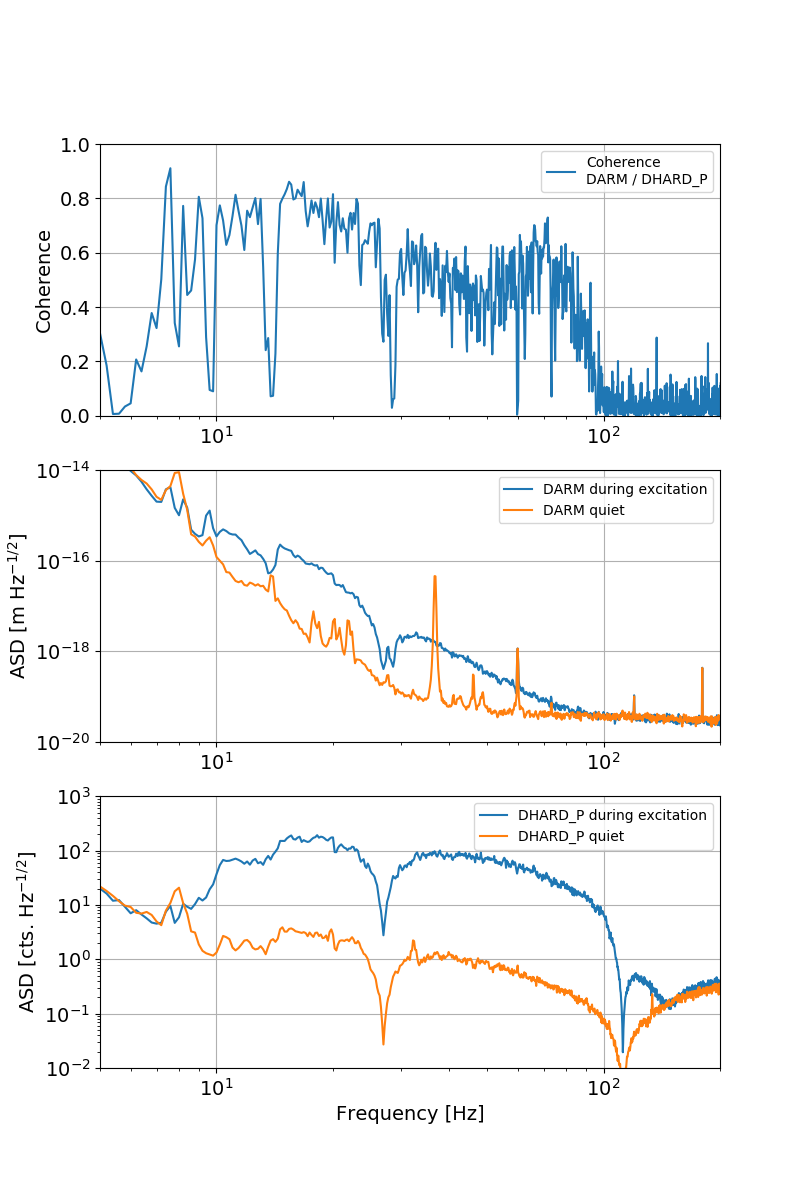
This is a follow-up on Sheila's alog about DHARD limiting the sensitivity (47209).
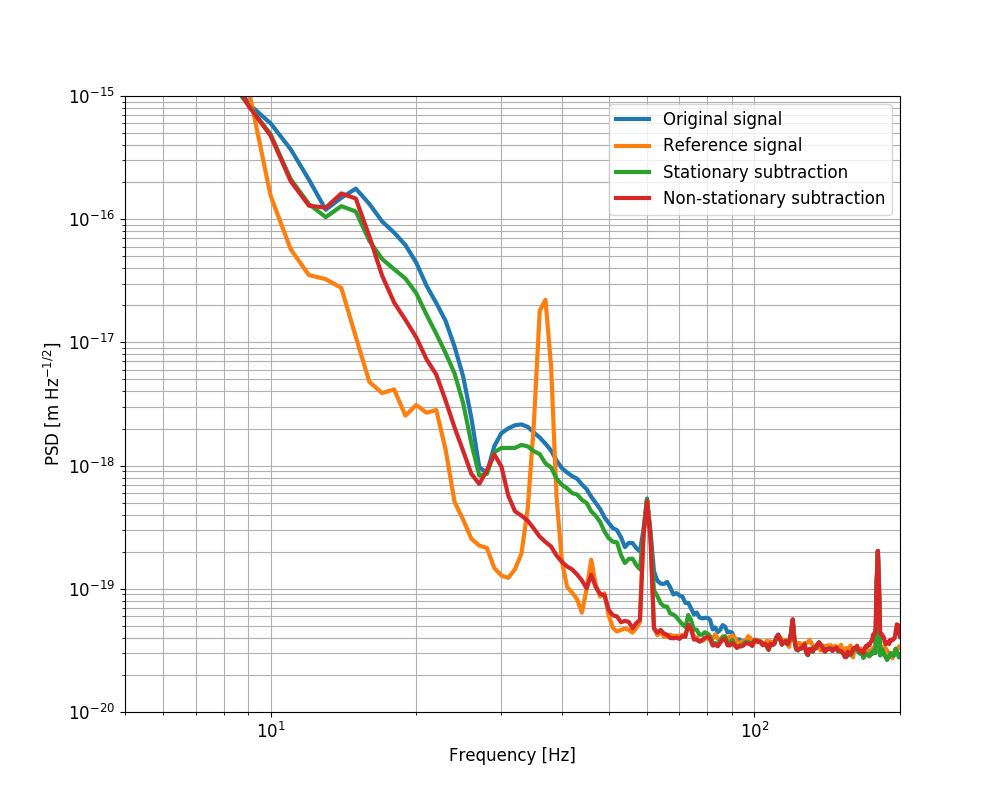
In summary: DHARD_P coupling to DARM is non stationary, we can subtract more with a non-stationary algorithm (at least during the noise injection, to be checked during quiet time)
The first evidence, as pointed out by Sheila, is that during a DHARD_P noise injection "the noise in DARM was increased by about a factor of 10-20 below 50Hz, but the coherence between DARM and the excitation is only around 0.7". The plot below shows the increase in DARM noise during the injection (note: I don't know what the line at 3X Hz is, probably my "quiet" time was during some other test) and how the coherence is too low, considering the SNR of the injection in both DARM and DHARD.
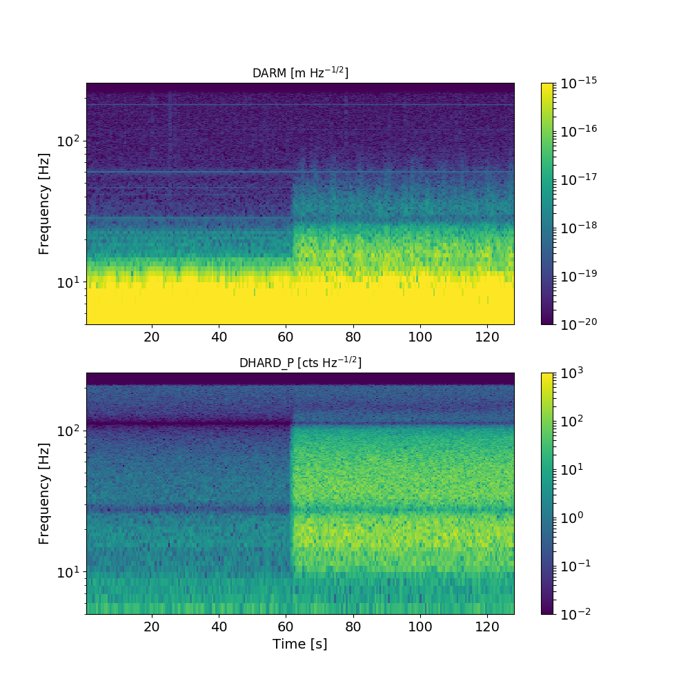
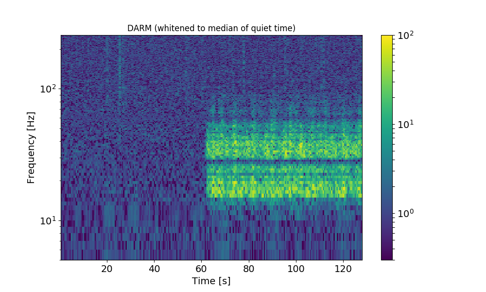
Another better evidence is provided by the spectrogram of DARM and DHARD around the injection time. The first figure below shows the DARM and DHARD signals when the noise injection is turned on (quiet time before t~=60s, DHARD_P injection for t>~60 s). DHARD_P is stationary, DARM is not. The second figure shows the DARM spectrogram, whitened to the median of the quiet time. The non-stationarity of the DARM noise is evident.
I used the non-stationary noise subtraction code described in many previous alogs for SRCL (45823 and links therein) and in all the details in T1800525. The noise witness channel is in this case ASC-DHARD_P_OUT_DQ, and the modulation channels are all the ASC input monitors. I used about 60 seconds of data during the DHARD_P noise injection (GPS = 1235434291 + 60s) to train the non-stationary model. For now the performance of the subtraction is shown on-target, meaning that I am using the same 60s to train and evaluate. There are other noise injections near that time and some quiet periods that I will later use.
First observation: the linear noise subtraction (green trace) does not perform very well, since it reduces the DHARD noise into DARM only by less than a factor 2. Second observation: the non-stationary noise subtraction (red trace), obtained by allowing the coupling to be modulated by the ASC input signals, performs much better at frequencies above 30 Hz, and slightly better at frequencies between 10 and 30 Hz. Not all DHARD noise is removed (compare red and orange).
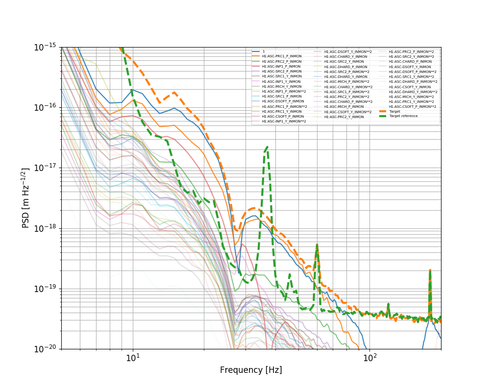
The plot below shows the main contribution to the noise subtraction, the main modulation coming from PRC1_P.
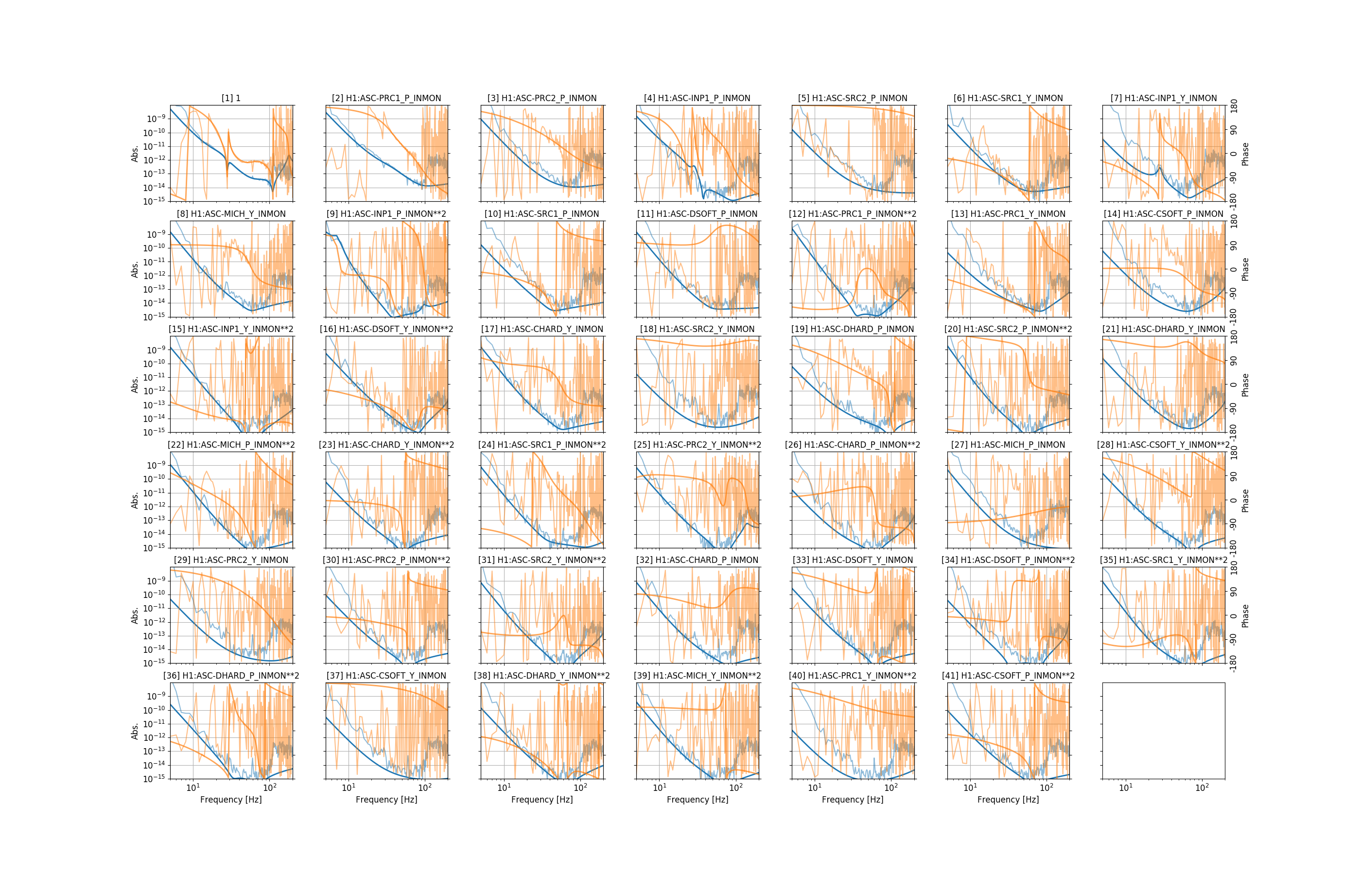
The last plot attached (not shown inline) contains all the coupling transfer functions.
H1tw3 (the new tw) is reporting a failed disk.
[530922.324644] sd 0:0:3:0: [sdd] Unhandled error code [530922.324649] sd 0:0:3:0: [sdd] [530922.324653] Result: hostbyte=DID_SOFT_ERROR driverbyte=DRIVER_OK [530922.324657] sd 0:0:3:0: [sdd] CDB: [530922.324661] Read(10): 28 00 3d 15 ab 68 00 00 80 00 [530922.324674] end_request: I/O error, dev sdd, sector 1024830312 [530922.833251] md/raid:md2: read error corrected (8 sectors at 1024830312 on sdd) [530922.833260] md/raid:md2: read error corrected (8 sectors at 1024830320 on sdd) [530922.833264] md/raid:md2: read error corrected (8 sectors at 1024830328 on sdd) [530922.833268] md/raid:md2: read error corrected (8 sectors at 1024830336 on sdd) [530922.833270] md/raid:md2: read error corrected (8 sectors at 1024830344 on sdd) [530922.833273] md/raid:md2: read error corrected (8 sectors at 1024830352 on sdd) [530922.833277] md/raid:md2: read error corrected (8 sectors at 1024830360 on sdd) [530922.833280] md/raid:md2: read error corrected (8 sectors at 1024830368 on sdd) [530922.833282] md/raid:md2: read error corrected (8 sectors at 1024830376 on sdd) [530922.833287] md/raid:md2: read error corrected (8 sectors at 1024830384 on sdd) [2037012.740535] md: data-check of RAID array md0 [2037012.740541] md: minimum _guaranteed_ speed: 1000 KB/sec/disk. [2037012.740544] md: using maximum available idle IO bandwidth (but not more than 200000 KB/sec) for data-check. [2037012.740551] md: using 128k window, over a total of 1950720k. [2037012.772561] md: delaying data-check of md1 until md0 has finished (they share one or more physical units) [2037012.786333] RAID conf printout: [2037012.786339] --- level:6 rd:6 wd:6 [2037012.786353] disk 0, o:1, dev:sda [2037012.786356] disk 1, o:1, dev:sdb [2037012.786358] disk 2, o:1, dev:sdc [2037012.786360] disk 3, o:1, dev:sdd [2037012.786362] disk 4, o:1, dev:sde [2037012.786364] disk 5, o:1, dev:sdf [2037012.786414] md: data-check of RAID array md2 [2037012.786418] md: minimum _guaranteed_ speed: 1000 KB/sec/disk. [2037012.786421] md: using maximum available idle IO bandwidth (but not more than 200000 KB/sec) for data-check. [2037012.786430] md: using 128k window, over a total of 512674304k. [2037022.277393] md: md0: data-check done. [2037022.281423] md: data-check of RAID array md1 [2037022.281427] md: minimum _guaranteed_ speed: 1000 KB/sec/disk. [2037022.281429] md: using maximum available idle IO bandwidth (but not more than 200000 KB/sec) for data-check. [2037022.281434] md: using 128k window, over a total of 242114560k. [2038242.597751] md: md1: data-check done. [2041160.323778] md: md2: data-check done. [2041160.335370] RAID conf printout: [2041160.335391] --- level:6 rd:6 wd:6 [2041160.335393] disk 0, o:1, dev:sda [2041160.335395] disk 1, o:1, dev:sdb [2041160.335397] disk 2, o:1, dev:sdc [2041160.335398] disk 3, o:1, dev:sdd [2041160.335400] disk 4, o:1, dev:sde [2041160.335401] disk 5, o:1, dev:sdf
To aid in finding it:
ata-Crucial_CT525MX300SSD1_1710162E56E0 -> ../../sdd
I'll check with Dave but we will probably take care of this during the daq downtime tomorrow.
/dev/sdd was not marked by the raid as failed. But with the errors in dmesg, we are going to pull it out and take a look at it. I have added the warm spare to the raid array, marked /dev/sdd as failed. We will pull the disk tomorrow when the daq is down so that we can test it out of line.
mdadm --add /dev/md2 /dev/sdo mdadm /dev/md2 --fail /dev/sddStatus:
mdadm --query --detail /dev/md2
/dev/md2:
Version : 1.2
Creation Time : Wed Feb 6 12:08:06 2019
Raid Level : raid6
Array Size : 2050697216 (1955.70 GiB 2099.91 GB)
Used Dev Size : 512674304 (488.92 GiB 524.98 GB)
Raid Devices : 6
Total Devices : 8
Persistence : Superblock is persistent
Intent Bitmap : Internal
Update Time : Mon Mar 4 14:13:49 2019
State : clean, degraded, recovering
Active Devices : 5
Working Devices : 7
Failed Devices : 1
Spare Devices : 2
Layout : left-symmetric
Chunk Size : 512K
Rebuild Status : 0% complete
Name : h1tw3:2 (local to host h1tw3)
UUID : 75304e90:3eaee815:04060b83:a8133c8b
Events : 945
Number Major Minor RaidDevice State
0 8 0 0 active sync /dev/sda
1 8 16 1 active sync /dev/sdb
2 8 32 2 active sync /dev/sdc
7 8 224 3 spare rebuilding /dev/sdo
4 8 64 4 active sync /dev/sde
5 8 80 5 active sync /dev/sdf
3 8 48 - faulty /dev/sdd
6 8 96 - spare /dev/sdg
As noted above, I marked sdd as failed, not the raid system.
The general query log had grown to 1.3 TB, so I turned it off and restarted both MySQL and conlog. The queue size is currently around 970,000 and growing. I'm not sure if it is going to drop to 0 or not. The list of added and removed channels is attached.
Turned conlog off. The queue size had no indication of dropping.
Averaging Mass Centering channels for 10 [sec] ...
2019-03-04 12:04:49.360399
There are 10 T240 proof masses out of range ( > 0.3 [V] )!
ETMX T240 1 DOF X/U = 0.412 [V]
ETMX T240 1 DOF Y/V = 0.317 [V]
ETMX T240 1 DOF Z/W = 0.419 [V]
ETMX T240 2 DOF X/U = -0.307 [V]
ETMX T240 2 DOF Y/V = -0.736 [V]
ETMX T240 3 DOF X/U = 0.345 [V]
ITMX T240 1 DOF X/U = -0.427 [V]
ITMX T240 3 DOF X/U = -0.373 [V]
ITMY T240 3 DOF Z/W = -0.59 [V]
BS T240 1 DOF Z/W = 0.31 [V]
All other proof masses are within range ( < 0.3 [V] ):
ETMX T240 2 DOF Z/W = 0.234 [V]
ETMX T240 3 DOF Y/V = 0.292 [V]
ETMX T240 3 DOF Z/W = 0.292 [V]
ETMY T240 1 DOF X/U = 0.085 [V]
ETMY T240 1 DOF Y/V = 0.264 [V]
ETMY T240 1 DOF Z/W = 0.107 [V]
ETMY T240 2 DOF X/U = 0.107 [V]
ETMY T240 2 DOF Y/V = 0.021 [V]
ETMY T240 2 DOF Z/W = 0.036 [V]
ETMY T240 3 DOF X/U = 0.115 [V]
ETMY T240 3 DOF Y/V = 0.107 [V]
ETMY T240 3 DOF Z/W = 0.289 [V]
ITMX T240 1 DOF Y/V = 0.165 [V]
ITMX T240 1 DOF Z/W = 0.138 [V]
ITMX T240 2 DOF X/U = 0.184 [V]
ITMX T240 2 DOF Y/V = 0.165 [V]
ITMX T240 2 DOF Z/W = 0.257 [V]
ITMX T240 3 DOF Y/V = 0.152 [V]
ITMX T240 3 DOF Z/W = 0.057 [V]
ITMY T240 1 DOF X/U = 0.217 [V]
ITMY T240 1 DOF Y/V = 0.142 [V]
ITMY T240 1 DOF Z/W = 0.192 [V]
ITMY T240 2 DOF X/U = 0.154 [V]
ITMY T240 2 DOF Y/V = 0.268 [V]
ITMY T240 2 DOF Z/W = 0.24 [V]
ITMY T240 3 DOF X/U = -0.092 [V]
ITMY T240 3 DOF Y/V = 0.23 [V]
BS T240 1 DOF X/U = 0.004 [V]
BS T240 1 DOF Y/V = -0.078 [V]
BS T240 2 DOF X/U = 0.079 [V]
BS T240 2 DOF Y/V = 0.29 [V]
BS T240 2 DOF Z/W = -0.02 [V]
BS T240 3 DOF X/U = 0.112 [V]
BS T240 3 DOF Y/V = -0.162 [V]
BS T240 3 DOF Z/W = -0.154 [V]
Assessment complete.
Averaging Mass Centering channels for 10 [sec] ...
2019-03-04 12:07:07.353372
There are 1 STS proof masses out of range ( > 2.0 [V] )!
STS A DOF X/U = -7.969 [V]
All other proof masses are within range ( < 2.0 [V] ):
STS A DOF Y/V = -0.922 [V]
STS A DOF Z/W = -0.258 [V]
STS B DOF X/U = 0.29 [V]
STS B DOF Y/V = -0.523 [V]
STS B DOF Z/W = -0.308 [V]
STS C DOF X/U = 0.358 [V]
STS C DOF Y/V = 0.165 [V]
STS C DOF Z/W = 0.645 [V]
STS EX DOF X/U = 0.026 [V]
STS EX DOF Y/V = 0.345 [V]
STS EX DOF Z/W = 0.317 [V]
STS EY DOF X/U = 0.359 [V]
STS EY DOF Y/V = -0.13 [V]
STS EY DOF Z/W = 0.793 [V]
Assessment complete.
Most of the T240 masses shown as out of range are on ETMX. I've now re-centered them, and all of the ETMX masses are currently back in spec. The other out of spec masses are only barely out of range and only one or two masses per chamber, so are not pressing.
Laser Status:
Front End Power is 32.1W (should be around 30 W)
70W Output Power is 70.84W
Front End Watch is GREEN
70W Watch is GREEN
PMC:
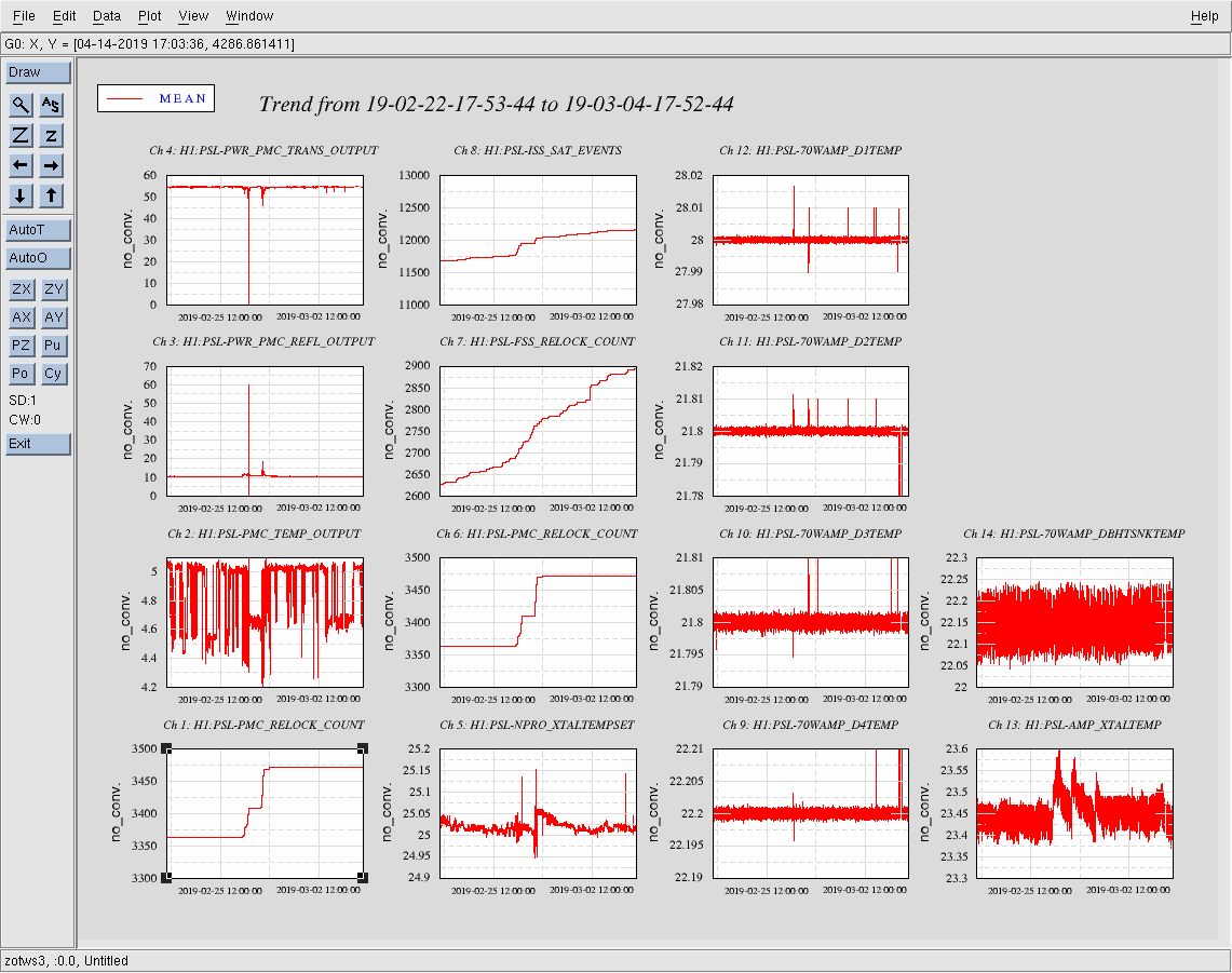
It has been locked 4 days, 20 hr 12 minutes (should be days/weeks)
Reflected power = 10.43Watts
Transmitted power = 54.54Watts
PowerSum = 64.97Watts.
FSS:
It has been locked for 0 days 0 hr and 16 min (should be days/weeks)
TPD[V] = 4.103V (min 0.9V)
ISS:
The diffracted power is around 2.4%
Last saturation event was 0 days 0 hours and 16 minutes ago (should be days/weeks)
Possible Issues:
Stefan, Peter, Rich It was found that the overall DC gain, and the pole-zero location associated with the second filter module of the OMC DCPD Whitening chain, was somehow dependent on input signal level. A parametric study was done on the OMC DCPD whitening chain for different whitening filter combinations with and without DC offset. Notes detailing the parametric study are attached to this entry. There were two causes of these phenomena: 1. Gain Change - As the DC input to the OMC DCPD Whitening amplifier (D1002559 Chassis S1101627) is varied, the DC level causes saturation in some of the DC coupled gain stages. This saturation causes the normally high-impedance amplifier input to be fairly low due current flowing into the input protection diodes internal to each opamp stage. This lower input resistance in conjunction with the series resistance of the FET switches produces a voltage divider with a division ratio dependent on signal level. 2. Pole-Zero Change - The second filter module had an ECR (E1500252) performed that required a 1uF capacitor to be used. This type of filter function is supposed to be implemented with a plastic film dielectric capacitor, but a ceramic capacitor was used instead. The piezoelectric nature of ceramic capacitors can result in a capacitance that will change with applied voltage. This caused the pole-zero location to vary as a function of DC level. This capacitor was changed to the proper type and the problem went away. Data (attached) was taken for both OMC DCPD chains by injecting signals into the input of the OMC whitening chassis (DCPD Preamps disconnected), and taking the output differentially from the analog output of the whitening chassis with the ADC cable still attached (to account for any loading effects). This data was taken with and without a 5V DC offset to verify that there is no longer any effect on the signal path gain. We note that the above were all small effects, but significant in the world of 1% calibratin uncertainty. The DC gain reduction with a 5 V offset (similar to the offset in NLN operation) was 0.2 dB. The errors in the filter stage with offset were -- phase: 0.6-1 degree at 50 Hz; magnitude: 0.15 dB gain difference between 50 Hz and 200 Hz.
Rich verbally confirms that he and Peter used the measurement setup as described in LHO aLOG 47225 and D1900027, using the coil driver test box as a differential driver. They *did not* gather the test setup's transfer function, however, so this will need to be done in order to analyze the data (attached above, DCPD_Whitening_v2.zip) to the desired precision. Also note that details of the measurement files can be found on the last page of the DCPDWhiteningChanges.pdf attachment. Also -- I opened (and subsequently closed) FRS Ticket 12453 covering the problem of "changes in frequency response as a result of input signal level" that the solution in this aLOG fixes. Since this issue will likely impact LLO as well, I've opened up an integration issue, IIET Ticket 12454, such that the above mentioned change becomes an ECR to be implemented at LLO as well (assuming they have the same problem).
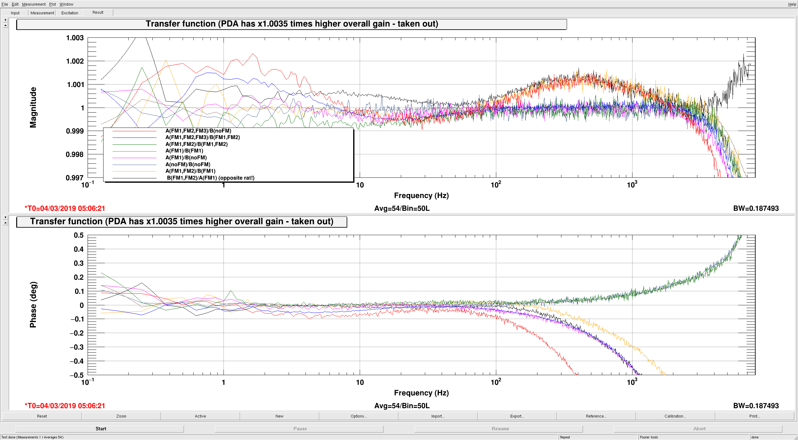
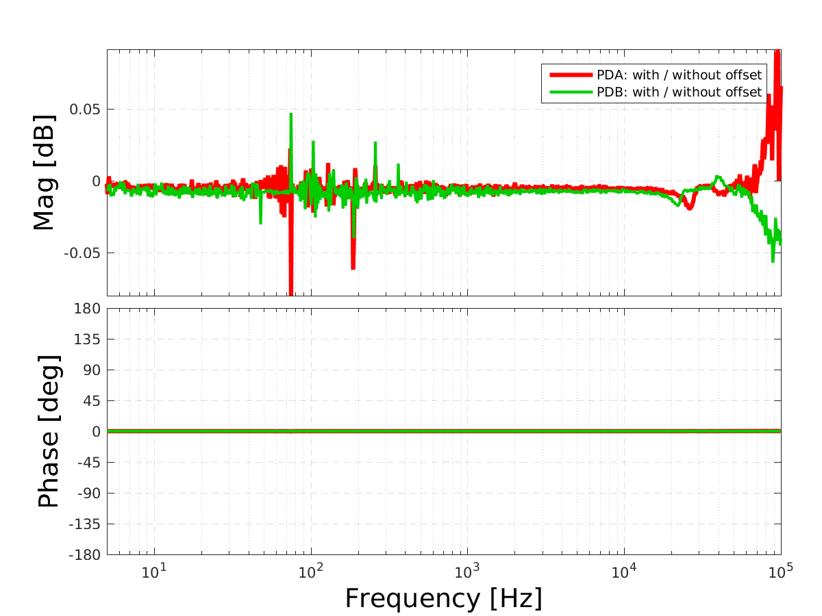
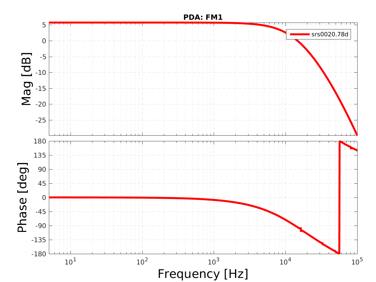
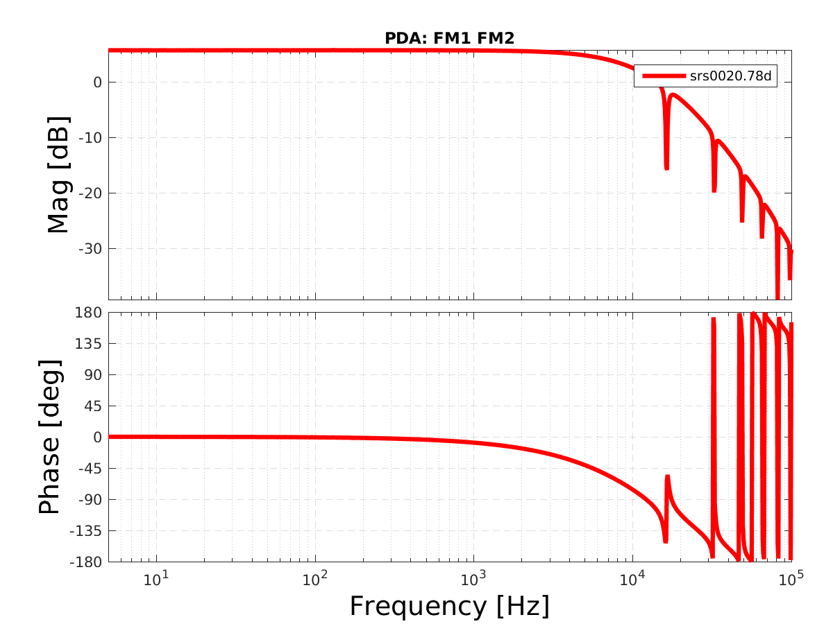
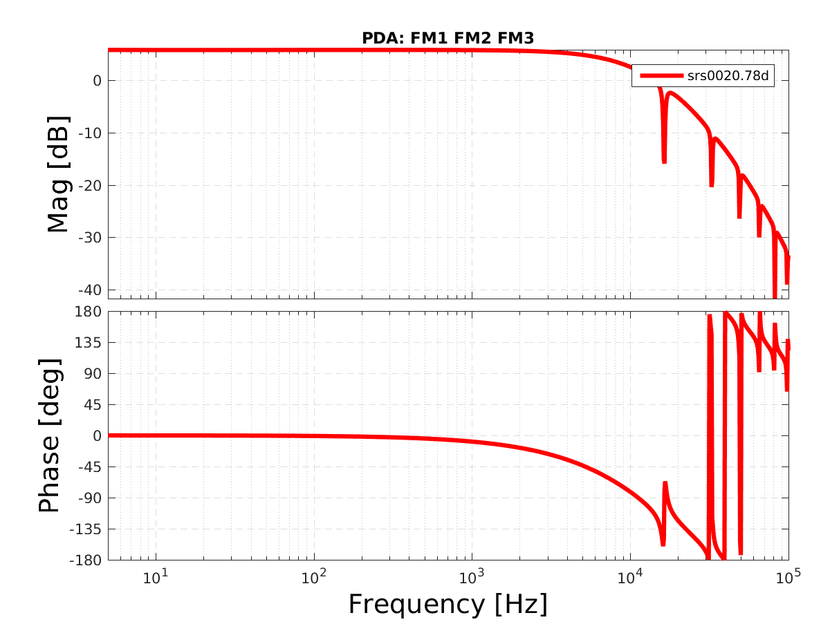
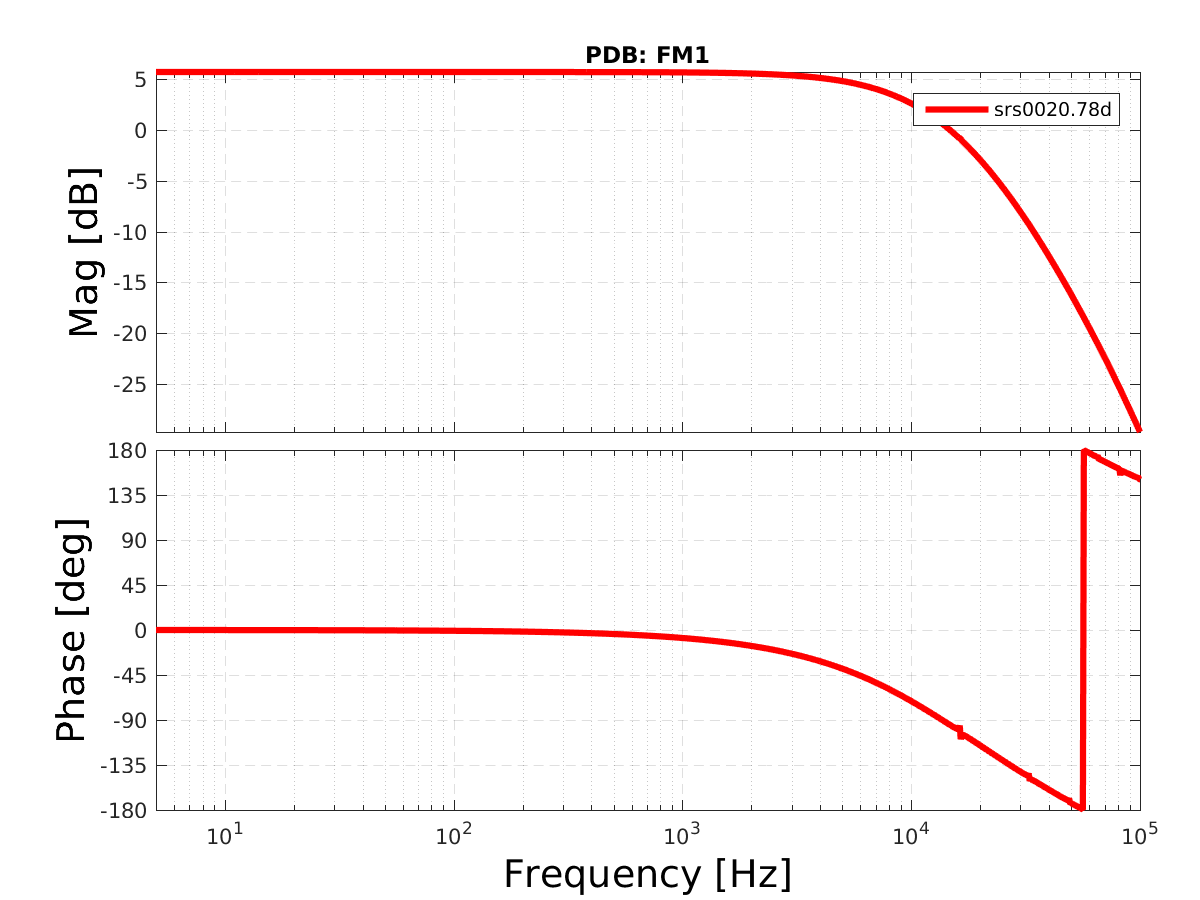
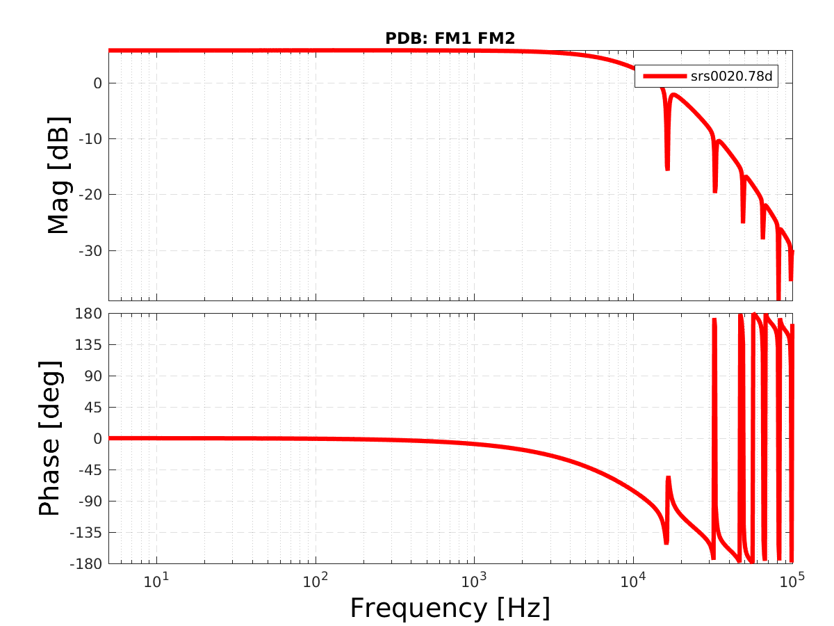
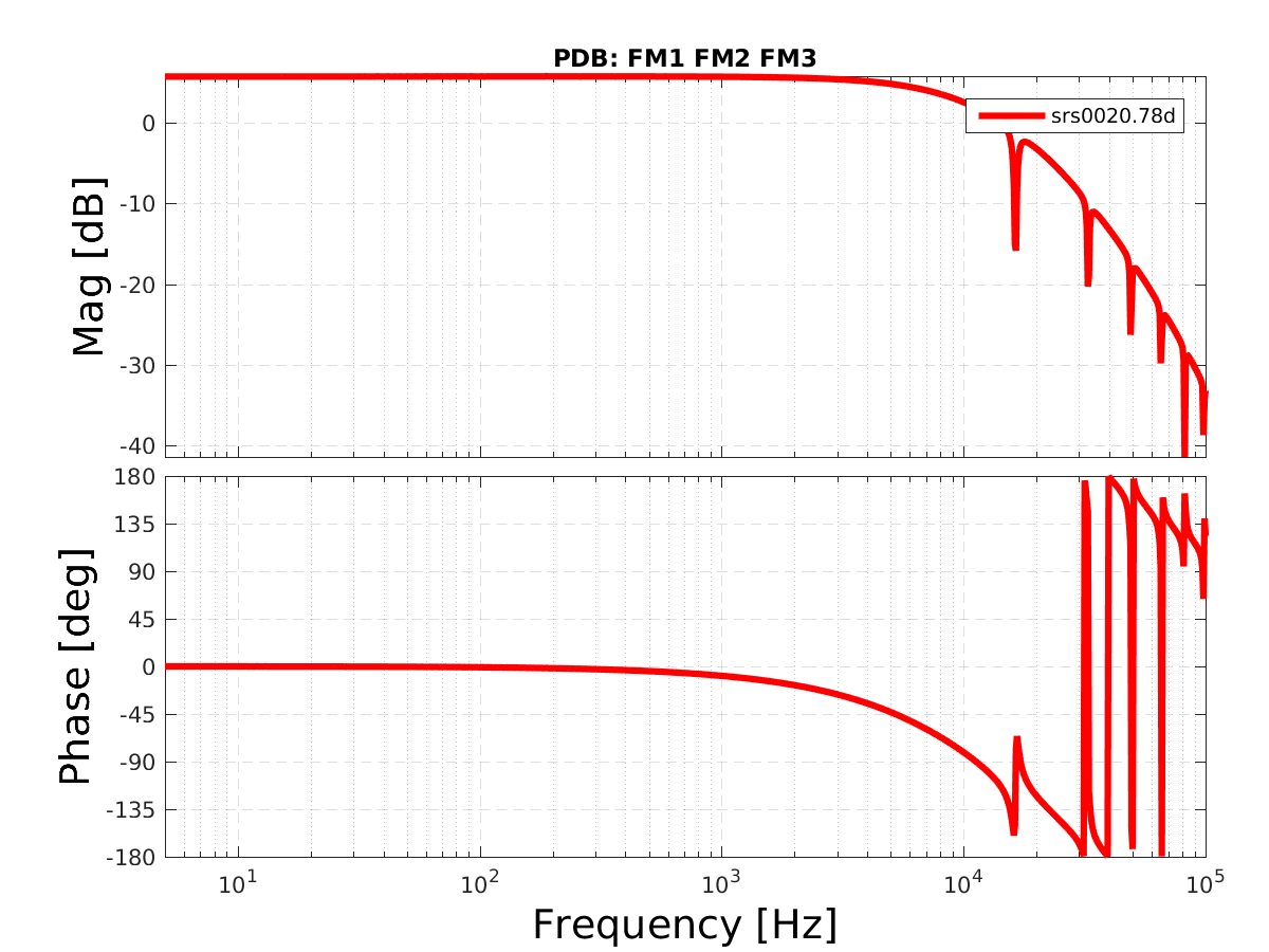
Updated the FM1,FM2,FM3 whitening compensation filters for PDA and PDB.
They are now matched at the +-0.15% level (see plot).
And we verified that they are no loner offset dependent.
Also, to be explicit: We disabled the 12dB, 6dB and 3dB whitening gain steps in both PDA and PDB. The 24dB step is still operational.
The new foton filters are:
PDA:
FM1: zpk([10.44],[0.996],0.9734,"n")
FM2: zpk([49.63],[497.5],-0.9995,"n")
FM3: zpk([10.372],[0.9865],1.002,"n")
PDB:
FM1: zpk([10.160],[0.969],0.975458,"n")
FM2: zpk([49.72],[497.7],-1.0004,"n")
FM3: zpk([10.467],[1.000],.9973,"n")
Using this filter, we injected pink noise into both DCPDs, and plotted the PD ratio in various configurations to verify the filter compensation. Specifically, plotted are:
A(FM1,FM2,FM3)/B(noFM)
A(FM1,FM2,FM3)/B(FM1,FM2)
A(FM1,FM2)/B(FM1,FM2)
A(FM1)/B(FM1)
A(FM1)/B(noFM)
A(noFM)/B(noFM)
A(FM1,FM2)/B(FM1)
B(FM1,FM2)/A(FM1) (opposite rat!)
The xml file with the data in the plot is in /ligo/home/controls/sballmer/20190303/DCPDfinal.xml
Finally, we still will have to re-match the photo diode light levels in lock (alog 47217).
All this was done to fix the problem identified in alog 47247.
Attached are plots of
- Transfer function wit- over-without offset. The insanity is indeed gone.
- PDA: FM1, FM1FM2, FM1FM2FM3 - all normalized with their compensation filter.
- PDB: FM1, FM1FM2, FM1FM2FM3 - all normalized with their compensation filter.
In short: the current compensation is good at the 0.02dB level. One could still improve it...
The plotting MATLAB code is here: /ligo/home/controls/sballmer/20190304/DCPD
I've moved the contents of Stefan's results from his home directory on the local file system into the calibration SVN (though I've not yet modified his plotting script for the new directories and/or to spit out the right file names).
I used the follow commands to do so:
Data:
cd /ligo/svncommon/CalSVN/aligocalibration/trunk/Common/Electronics/H1/Data/OMCWhiteningChassis/2019-03-04/
cp /ligo/home/controls/sballmer/20190304/DCPD/SRS00* ./
cp /ligo/home/controls/sballmer/20190304/DCPD/srs00* ./
cp /ligo/home/controls/sballmer/20190304/DCPD/47254_20190303213* ./
Script:
cd /ligo/svncommon/CalSVN/aligocalibration/trunk/Common/Electronics/H1/Scripts/
cp /ligo/home/controls/sballmer/20190304/DCPD/plotData.m plot_omcdcpdwhiteningmods_20190304.m
Results:
cd /ligo/svncommon/CalSVN/aligocalibration/trunk/Common/Electronics/H1/Results/OMCWhiteningChassis/
cp /ligo/home/controls/sballmer/20190304/DCPD/PD*.png ./
rename 's/PD/2019-03-04\_H1OMC\_WhiteningChassisTFs\_PD/' PD*.png
Thus the new script name to plot the data is:
/ligo/svncommon/CalSVN/aligocalibration/trunk/Common/Electronics/H1/Scripts/plot_omcdcpdwhiteningmods_20190304.m
which should be modified to analyze the following data:
/ligo/svncommon/CalSVN/aligocalibration/trunk/Common/Electronics/H1/Data/OMCWhiteningChassis/2019-03-04/
SRS00*.78D
srs00*.asc
using the notes in the file
/ligo/svncommon/CalSVN/aligocalibration/trunk/Common/Electronics/H1/Data/OMCWhiteningChassis/2019-03-04/
47254_20190303213544_DCPDWhiteningChanges.pdf
and to produce plots and results with similar file tags as
/ligo/svncommon/CalSVN/aligocalibration/trunk/Common/Electronics/H1/Results/OMCWhiteningChassis/
2019-03-04_H1OMC_WhiteningChassisTFs_PD*.png
(or the code should be re-written to use your favorite fitting code [maybe in python using IIRrational] and produce plots and results with similarly explicit file names with indications of the date, the interferometer, and WhiteningChassisTFs in the file name.)
Lilli S.,
First, I have renamed the data files in dir /ligo/svncommon/CalSVN/aligocalibration/trunk/Common/Electronics/H1/Data/OMCWhiteningChassis/2019-03-04/, so that they match what is described in note /ligo/svncommon/CalSVN/aligocalibration/trunk/Common/Electronics/H1/Data/OMCWhiteningChassis/2019-03-04/47254_20190303213544_DCPDWhiteningChanges.pdf
The test box has been factored out. (Test box data: /ligo/svncommon/CalSVN/aligocalibration/trunk/Common/Electronics/H1/Data/CoilDriverTestBox/S1900070/)
The fitting script is /ligo/svncommon/CalSVN/aligocalibration/trunk/Common/Electronics/H1/Scripts/fit_OMCDCPDWhiteningChassis_20190304.py
The results are in the table below. The fitting plots are in the attachments.
The low-freq poles/zeros roughly match Stefan's results. In O1 and O2 we used 1 stage of whitening (FM1), and the high freq poles were at [(14.34e3 + 14.60e3)/2, (18.68e3 + 18.57e3)/2, (98.94e3 + 100.45e3)/2] Hz. The new fitting for FM1 is consistent with O1 and O2.
Take PDA FM1FM2FM3 noDC as an example, manually build TF by removing the high-freq zeros, and plot the residual -> see diff.pdf
By ignoring the high-freq zeros, there's little impact on magnitude, but there's phase difference at higher freq (~<1 deg below 5k Hz).
| PDA | PDB | Comments | |
| FM1FM2FM3 (no DC) | PDA, Filters: FM1FM2FM3noDC Results: z:p:k [ 3.90426349e+06 3.90426349e+06 4.99892253e+02 1.08290122e+00 1.08040698e+00] [ 1.04233314e+01 3.26866242e+04 3.26866242e+04 1.13980014e+04 4.97078295e+01 1.04233314e+01] -8.68011786846 |
PDB, Filters: FM1FM2FM3noDC Results: z:p:k [ 4.64029327e+06 4.64029327e+06 5.00447159e+02 1.07523773e+00 1.07282309e+00] [ 1.03389750e+01 3.28642175e+04 3.28642175e+04 1.15193027e+04 1.03389750e+01 4.97939024e+01] -6.26981682358 |
Low-freq zeros near 1Hz, 1Hz, 500Hz, and poles near 10Hz, 10Hz, 50Hz (as expected) High-freq poles near 12K, 33K, 33K Hz. |
| FM1FM2FM3 (4.99V DC) | PDA, Filters: FM1FM2FM3DC Results: z:p:k [ 4.83659991e+06 4.83659991e+06 4.99682906e+02 1.08106936e+00 1.08299624e+00] [ 1.04231076e+01 3.28748478e+04 3.28748478e+04 1.13460627e+04 1.04231076e+01 4.96890494e+01] -5.6929144981 |
PDB, Filters: FM1FM2FM3DC Results: z:p:k [ 3.93271594e+06 3.93271594e+06 5.00449636e+02 1.07585358e+00 1.07328174e+00] [ 4.98000266e+01 3.28631506e+04 3.28631506e+04 1.15205406e+04 1.03375026e+01 1.03375026e+01] -8.72188264417 |
Low-freq zeros near 1Hz, 1Hz, 500Hz, and poles near 10Hz, 10Hz, 50Hz (as expected) High-freq poles near 12K, 33K, 33K Hz. |
| FM1FM2 (no DC) |
PDA, Filters: FM1FM2 Results: z:p:k |
PDB, Filters: FM1FM2 Results: z:p:k [ 2.11805525e+06 8.72055868e+05 5.00733633e+02 1.14755102e+00] [ 2.04506589e+04 1.24360067e+04 8.94998324e+04 4.97729997e+01 1.02056871e+01] -12.7328787001 |
Low-freq zeros near 1Hz, 500Hz, and poles near 10Hz, 50Hz (as expected) High-freq poles near 12K, 20K, 89K Hz. |
| FM1 (no DC) | PDA, Filters: FM1 Results: z:p:k [ 4.22938089e+06 4.22938089e+06 1.17507390e+00] [ 1.27384958e+04 1.93716076e+04 9.29113659e+04 1.04895576e+01] 13.3497796427 |
PDB, Filters: FM1 Results: z:p:k [ 4.84207436e+06 4.84207436e+06 1.14699930e+00] [ 1.29122349e+04 1.93696499e+04 9.46279852e+04 1.02067553e+01] 10.4974545401 |
Low-freq zeros near 1Hz and poles near 10Hz (as expected) High-freq poles near 13K, 19K, 93K Hz. |
| noFM (no DC) | PDA, Filters: noFM Results: z:p:k [ 1.26091781e+07 3.57048935e+07 2.05610666e-01] [ 1.28075383e+04 1.92624890e+04 1.84656469e+06 4.98134421e-02] 0.980629117874 |
PDB, Filters: noFM Results: z:p:k [ 2.82948542e+07 2.84161583e+07 2.05615042e-01] [ 1.29617754e+04 1.93273505e+04 2.08761329e+06 4.98133861e-02] 0.629314166113 |
High-freq poles near 13K, 19K Hz. Unphysical low-freq zero near 0.2Hz and pole near 0.05Hz. |
Concluding from the results of the fit above, I'll be updating the calibration model parameters to change from the previous measurement of the DCPD whitening chassis (before O2, when the nominal configuration was to only have the first stage of whitening -- "F1" or "FM1" -- on; see LHO aLOG 28087) from PDA PDB PDA PDB PDA PDB uncompOMCpoles_whitening = [(14.34e3 + 14.60e3)/2, (18.68e3 + 18.57e3)/2, (98.94e3 + 100.45e3)/2]; to the new fitted measurement results, and choosing the new nominal configuration, with all three filters on (the 1st and 3rd stages, which are whitening and the 2nd stage which is a low pass, i.e. "FM1FM2FM3" or "3 filt"), and using the 5 V_DC offset fit results because it's more representative of the nominal running conditions of the chassis (with the poles rounded to the nearest Hz) PDA PDB PDA PDB PDA PDB uncompOMCpoles_whitening = [(11.346e3 + 11.521e3)/2, (32.875e3 + 32.863e3)/2, (32.875e3 + 32.863e3)/2];
Lilli S.,
The residual contribution plot is attached. This was generated using /ligo/svncommon/CalSVN/aligocalibration/trunk/Common/Electronics/H1/Scripts/fit_OMCDCPDWhiteningChassis_20190304-vsOriginal.py
(based on reference model modelparams_H1_20190118)
The results is averaged after using different poles/zeros in PDA and PDB, instead of using the same set of averaged poles/zeros in PDA and PDB.
Per Jeff's request that the original DCPD files be included, I am attaching the data extending down to 0.5Hz for the OMC DCPD Whitening chain as taken on the floor by signal injection into the front panel of the Split Whitening Chain via an SR785
Attached are two plots:
A) The comparison of TFs:
1. All low-freq z:p + high-freq p + out-of-band z from IIRrational fitting
2. Dead reckoned z:p = [500, 1, 1]:[50, 10, 10]
3. Low-freq z:p from Stefan's fitting in 47257
4. Low-freq z:p from Stefan's fitting in 47257 + high-freq p from IIRational
B) The comparison of contribution residuals, by using the latest H1 model 20190301
The scripts live in
/ligo/svncommon/CalSVN/aligocalibration/trunk/Common/Electronics/H1/Scripts/fit_OMCDCPDWhiteningChassis_20190304-compareTF.py
/ligo/svncommon/CalSVN/aligocalibration/trunk/Common/Electronics/H1/Scripts/fit_OMCDCPDWhiteningChassis_20190304-compareRes.py
Craig, Rich, Peter, Stefan,
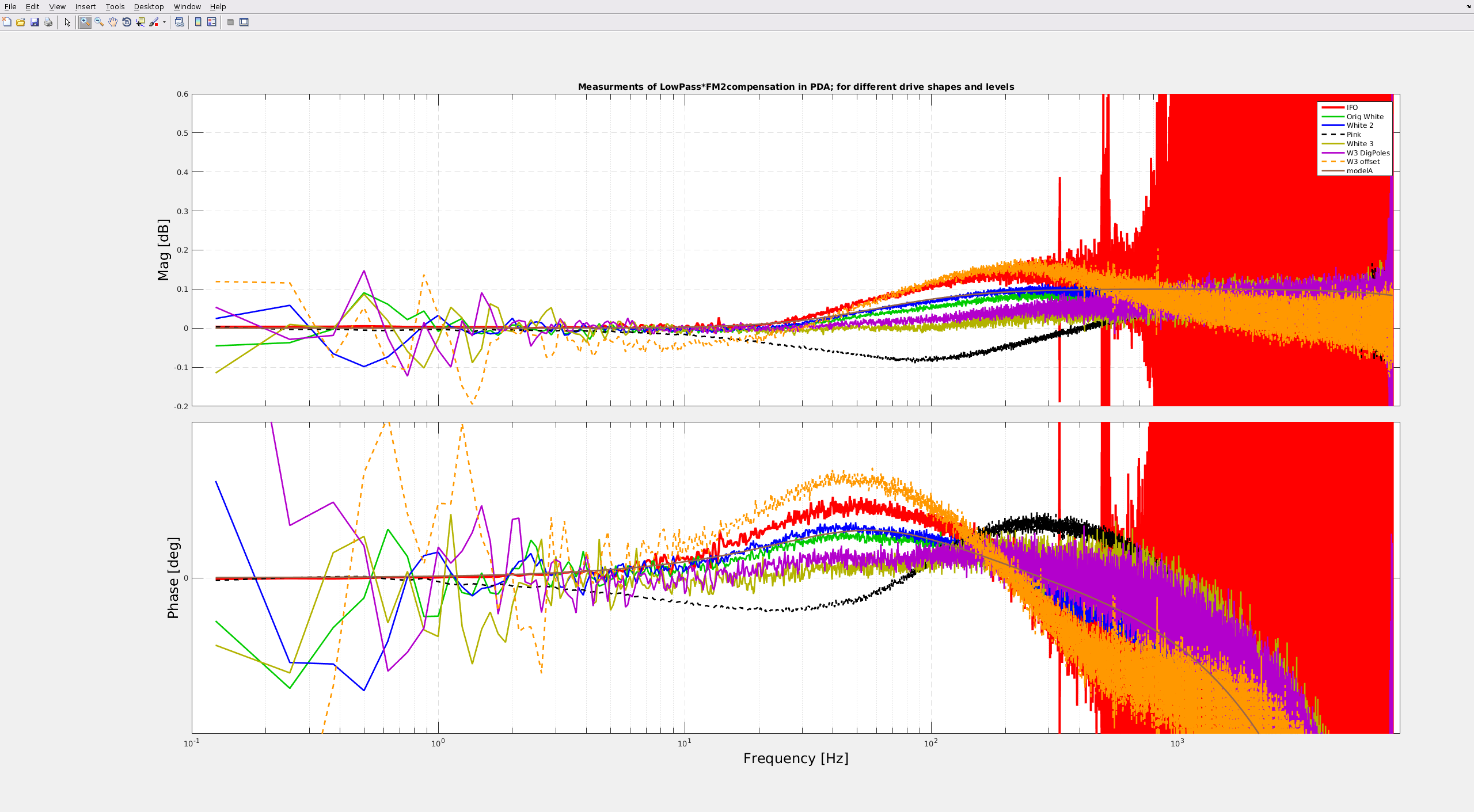
We tried to measure and fine-tune the DCPD whitening filter compensation. so we took the following measurments:
a) Analog transfer function on the floor for PDA & PDB; FM1FM2FM3 all off and FM1FM2FM3 all on (run configuration). (That's 4 measurements total.) That data is still on disk and Rich will post it.
b) Driving both DCPDs with noise, measure the PDA/PDB transfer function. This is done with FM1&FM2 on PDA and FM1 on PDB, normalized by FM1 on PDA and FM1 on PDB to take out other systematics.
Measurement b) was performed with a variety of noise sources:
i) IFO on AS_RF45, with additional 100Hz-1kHz frequency noise injection. (IFO)
ii) White noise drive (10Vpkk) (Orig white)
iii) Same white noise, but FM6 filters in PDA and PDB off (White 2). Note that changed the transfer function at the 1e-3 level compared with ii) - consistent with T990013-B (dtt documentation)
iv) Same white noise, but now filtered by SR560 with 2 poles at 100Hz (Pink)
v) White noise at half the level (5Vpkk) (White 3)
vi) Same as white 3, but with 2 poles at 100Hz in the digital system (W3 Dig Poles)
vii) Same as white 3, but additional 2V offset (~13000cts at IN1) (W3 offset)
viii) Simple model z59.8265:p60.174,120k
Note that at 100Hz the transfer function is changing by as much as 0.3dB (3.5%) with drive level..THis is much bigger than the expected dtt error, so we conclude it is real, We will deal with the implications for calibration tomorrow.
I attach the data taken with the SR785 on the DCPD Whitening chain.
Problem fixed in alog 47254.
I opened (and subsequently closed) FRS Ticket 12453 that corresponds to this issue. As Stefan mentions, the solution has already been implemented (and will likely become an ECR to change all OMC DCPD whitening chassis).
Peter F., Rich A., Daniel, Nutsinee
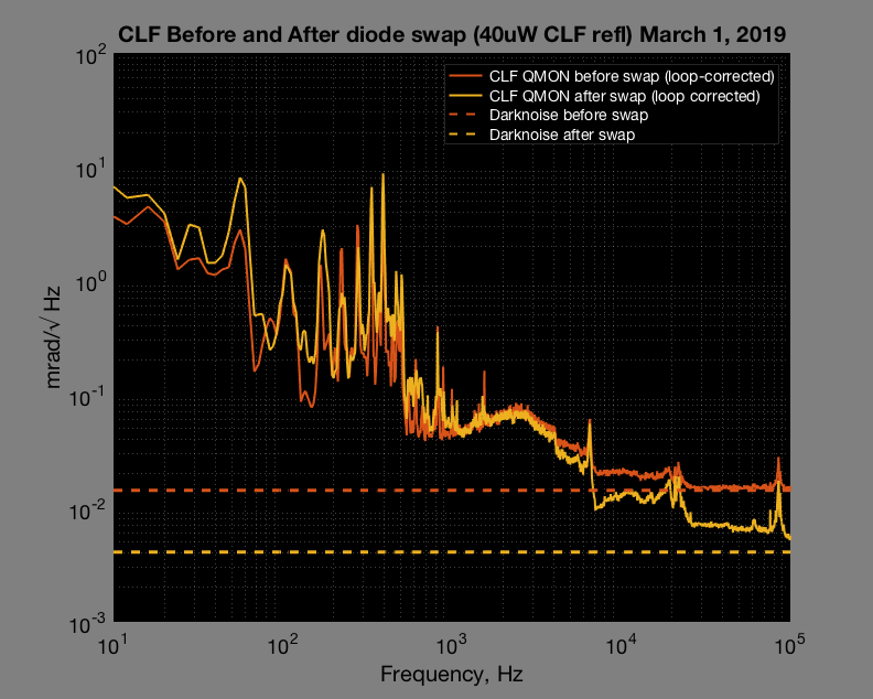
The dark noise is factor of 3.75 better with the new diode. With this we can crank up the loop UGF as high as we could to squash the acoustic noise (and some of the stuff above 1kHz). We can also try operating at lower CLF power. With both of these things we should gain a bit more squeezing.
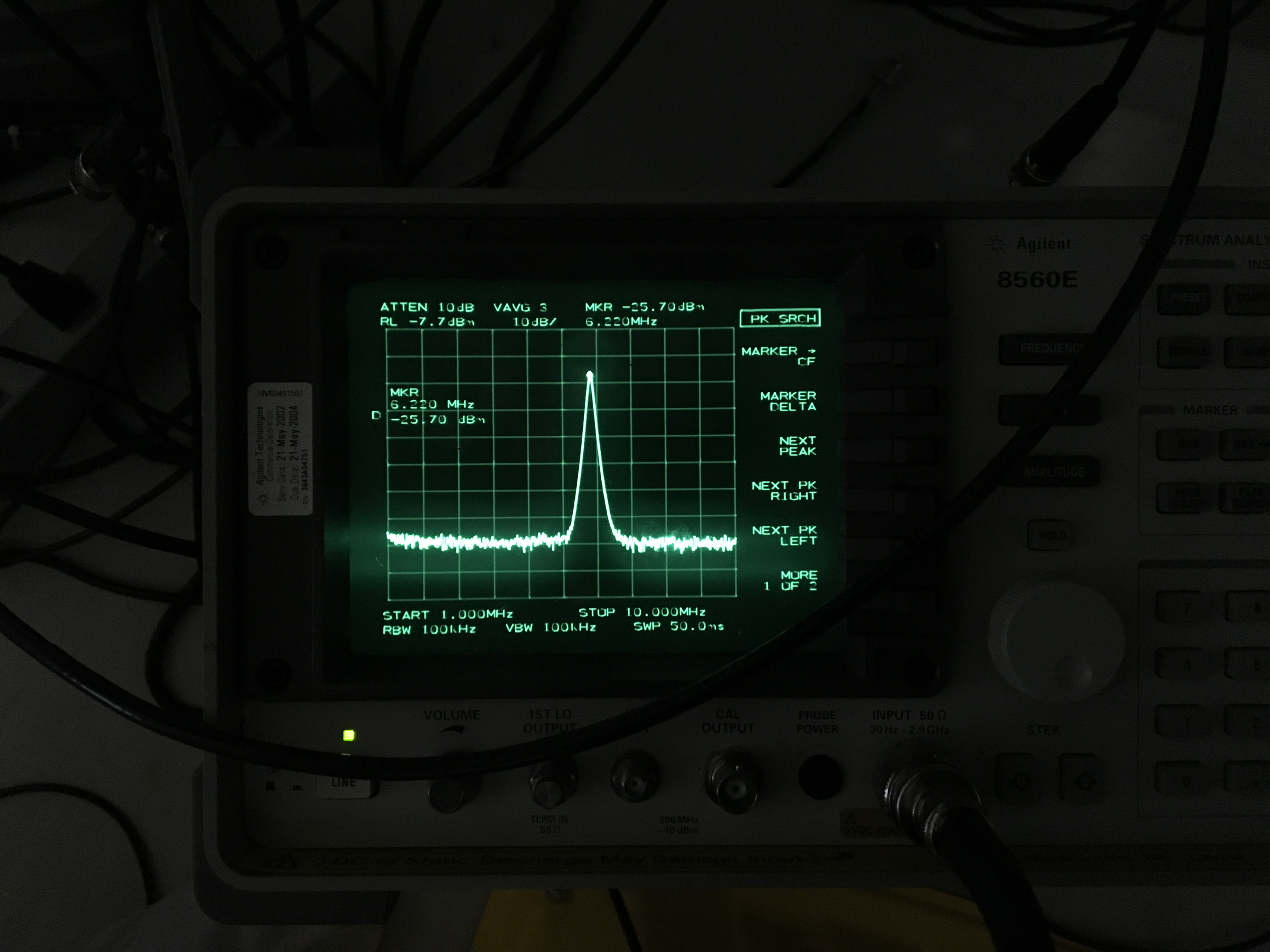
Compared to the old diode we gained 8dB of RF power. More information about the new diode can be found in alog47171 and alog47196.
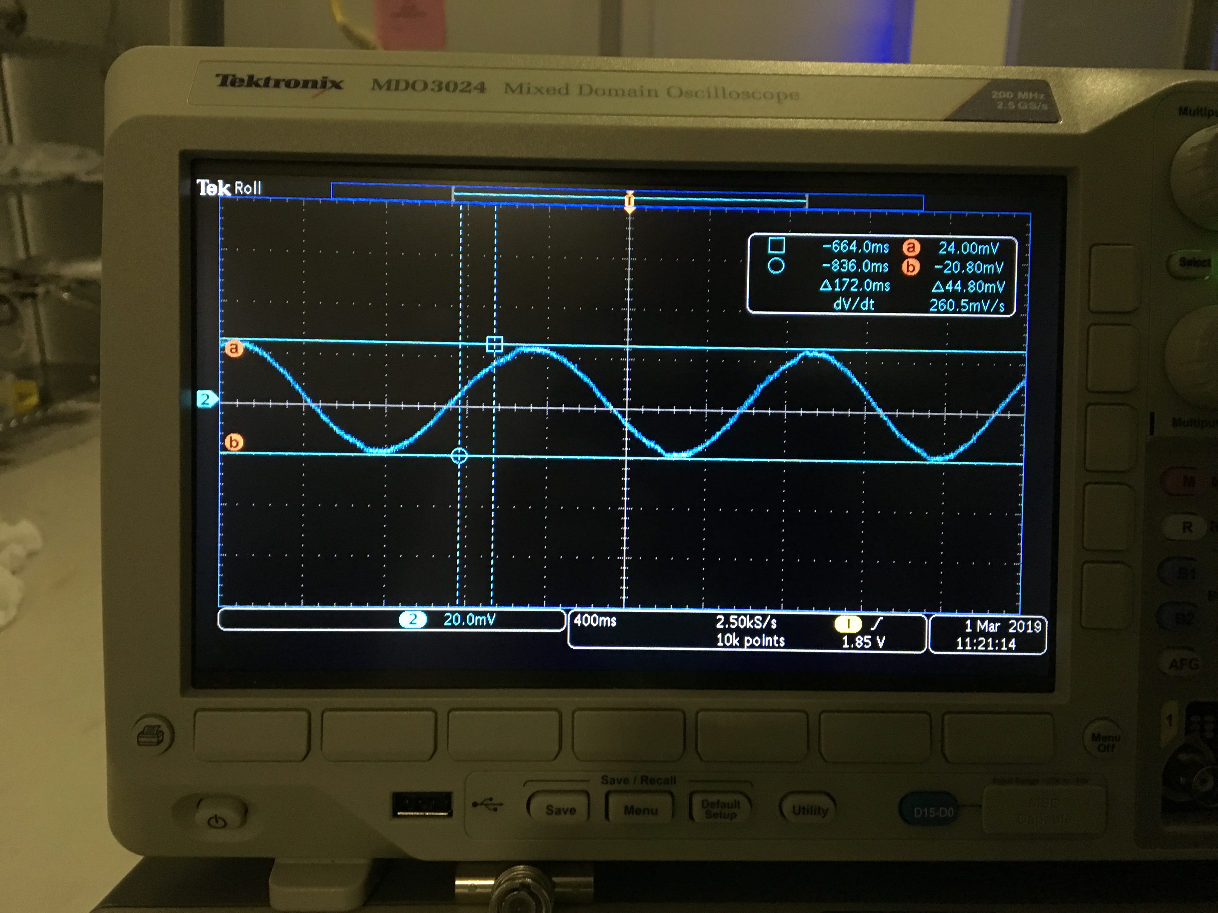
Also attached RF beat note and the sine wave from the IQ demod board RF mon (23dB attenuated).

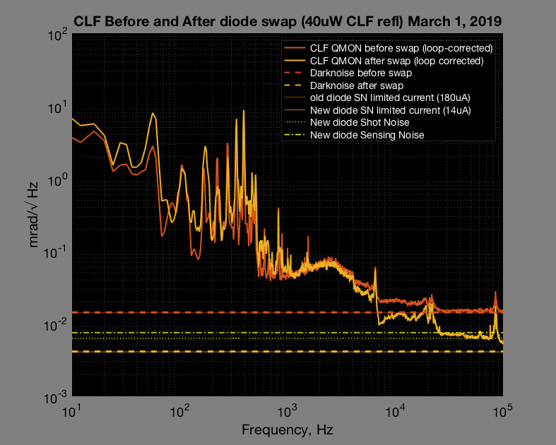
Attached the same plot but with sensing noise. Using a shot noise measurement from the light bulb and a DC transimpedance of 10kOhms we got a RF transimpedance of 1.87kOhms for the new detector. For the old detector I got 678.8 Ohms transimpedance. This factor of ~3 seems to explain then amount of RF power we get before and after the swap.
A factor of 25 (RF amp) *sqrt(2) (SN folded in IQdemod) * 5(IQdemod board gain) * 10(diode gain) have been included for both cases.

In the above plot it seems that the measured noise is below the sensing noise at 100kHz. This effect is due to the ~100kHz bandwidth of the photodiode (Q~30 at 6.25MHz).
Removing the diode gain, we have an overall RF transimpedance gain of 6.8kOhm and 18.7kOhm for the old and new photodiode, respectively. The second stage gains are 50 and 5, respectively. This leaves a gain of 140Ohm and 3.7kOhm in the first stage, respectively. So, we may expect an improvement of the dark noise by ~5.