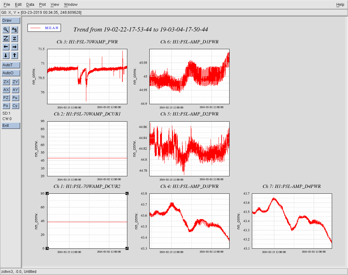
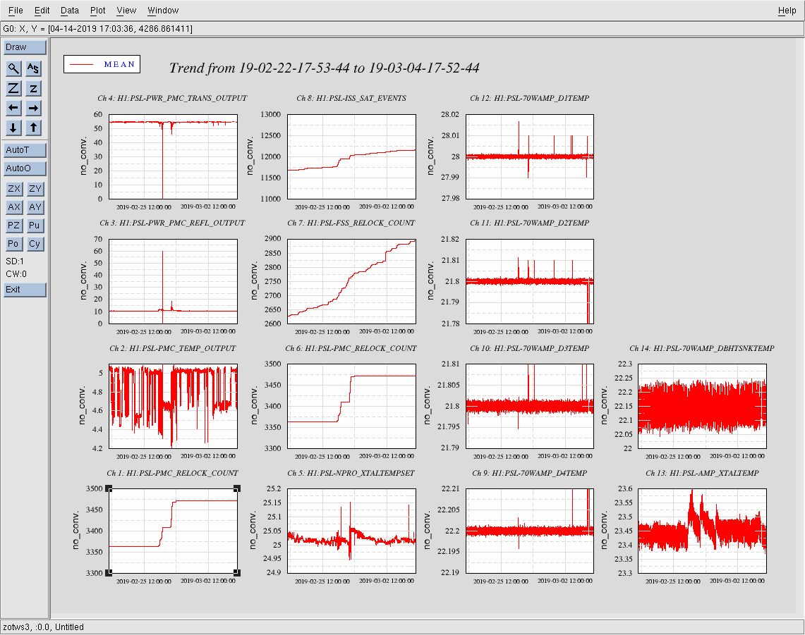
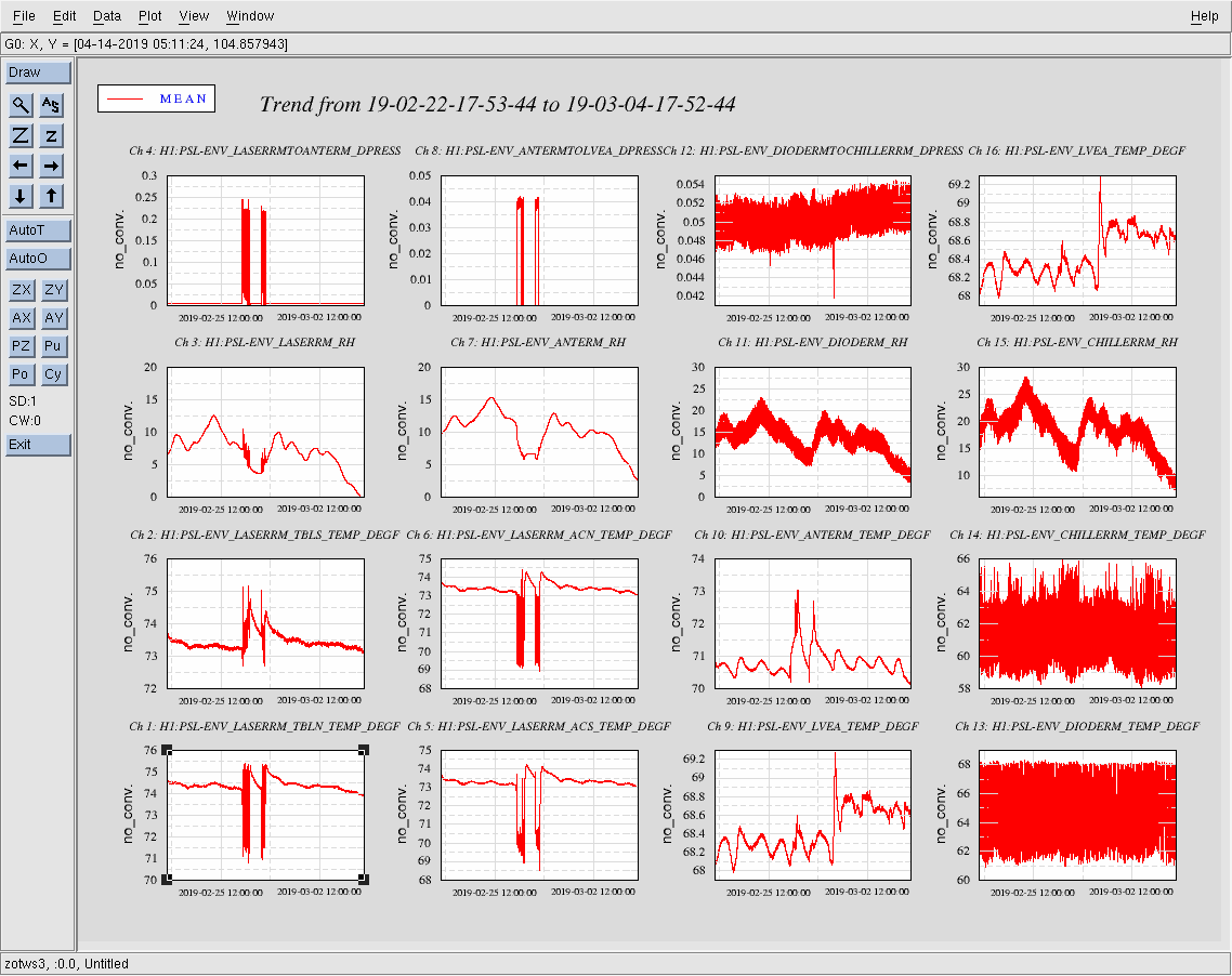
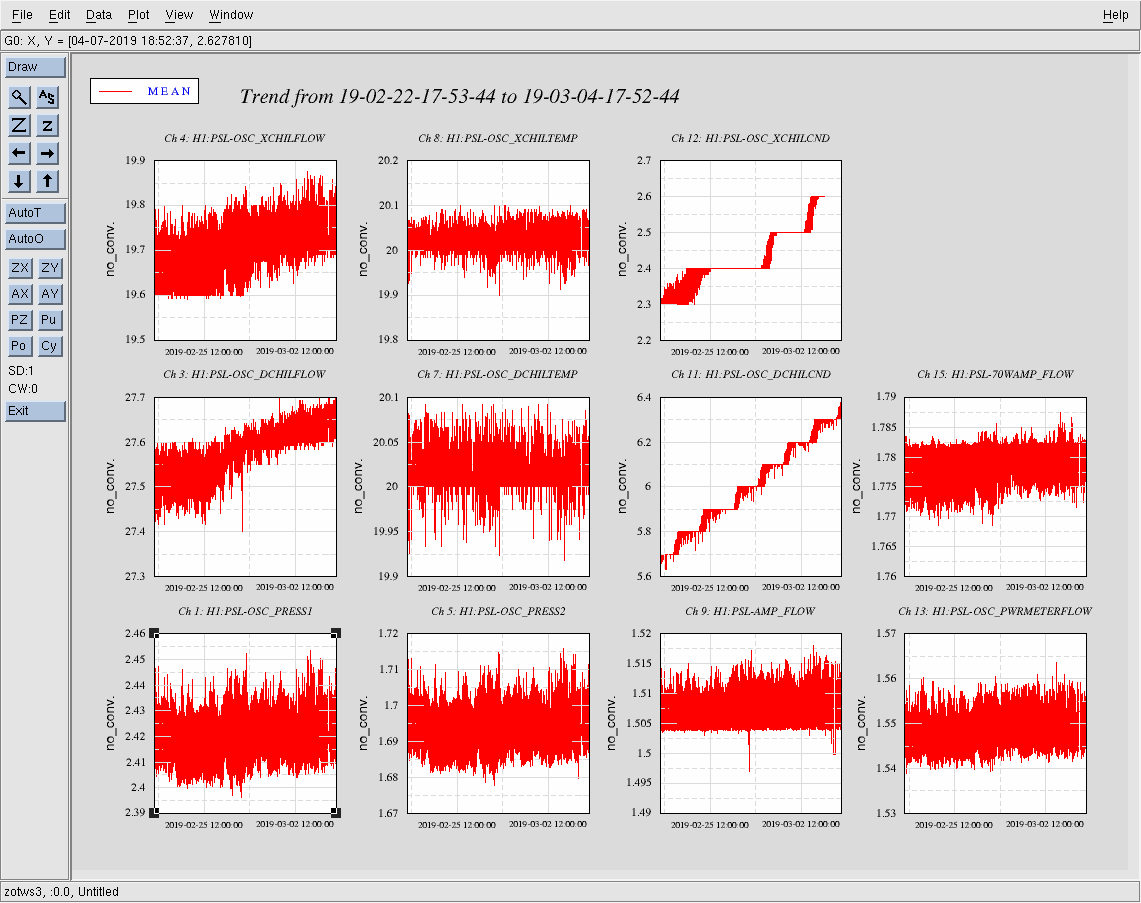
The general query log had grown to 1.3 TB, so I turned it off and restarted both MySQL and conlog. The queue size is currently around 970,000 and growing. I'm not sure if it is going to drop to 0 or not. The list of added and removed channels is attached.
Turned conlog off. The queue size had no indication of dropping.
Averaging Mass Centering channels for 10 [sec] ...
2019-03-04 12:04:49.360399
There are 10 T240 proof masses out of range ( > 0.3 [V] )!
ETMX T240 1 DOF X/U = 0.412 [V]
ETMX T240 1 DOF Y/V = 0.317 [V]
ETMX T240 1 DOF Z/W = 0.419 [V]
ETMX T240 2 DOF X/U = -0.307 [V]
ETMX T240 2 DOF Y/V = -0.736 [V]
ETMX T240 3 DOF X/U = 0.345 [V]
ITMX T240 1 DOF X/U = -0.427 [V]
ITMX T240 3 DOF X/U = -0.373 [V]
ITMY T240 3 DOF Z/W = -0.59 [V]
BS T240 1 DOF Z/W = 0.31 [V]
All other proof masses are within range ( < 0.3 [V] ):
ETMX T240 2 DOF Z/W = 0.234 [V]
ETMX T240 3 DOF Y/V = 0.292 [V]
ETMX T240 3 DOF Z/W = 0.292 [V]
ETMY T240 1 DOF X/U = 0.085 [V]
ETMY T240 1 DOF Y/V = 0.264 [V]
ETMY T240 1 DOF Z/W = 0.107 [V]
ETMY T240 2 DOF X/U = 0.107 [V]
ETMY T240 2 DOF Y/V = 0.021 [V]
ETMY T240 2 DOF Z/W = 0.036 [V]
ETMY T240 3 DOF X/U = 0.115 [V]
ETMY T240 3 DOF Y/V = 0.107 [V]
ETMY T240 3 DOF Z/W = 0.289 [V]
ITMX T240 1 DOF Y/V = 0.165 [V]
ITMX T240 1 DOF Z/W = 0.138 [V]
ITMX T240 2 DOF X/U = 0.184 [V]
ITMX T240 2 DOF Y/V = 0.165 [V]
ITMX T240 2 DOF Z/W = 0.257 [V]
ITMX T240 3 DOF Y/V = 0.152 [V]
ITMX T240 3 DOF Z/W = 0.057 [V]
ITMY T240 1 DOF X/U = 0.217 [V]
ITMY T240 1 DOF Y/V = 0.142 [V]
ITMY T240 1 DOF Z/W = 0.192 [V]
ITMY T240 2 DOF X/U = 0.154 [V]
ITMY T240 2 DOF Y/V = 0.268 [V]
ITMY T240 2 DOF Z/W = 0.24 [V]
ITMY T240 3 DOF X/U = -0.092 [V]
ITMY T240 3 DOF Y/V = 0.23 [V]
BS T240 1 DOF X/U = 0.004 [V]
BS T240 1 DOF Y/V = -0.078 [V]
BS T240 2 DOF X/U = 0.079 [V]
BS T240 2 DOF Y/V = 0.29 [V]
BS T240 2 DOF Z/W = -0.02 [V]
BS T240 3 DOF X/U = 0.112 [V]
BS T240 3 DOF Y/V = -0.162 [V]
BS T240 3 DOF Z/W = -0.154 [V]
Assessment complete.
Averaging Mass Centering channels for 10 [sec] ...
2019-03-04 12:07:07.353372
There are 1 STS proof masses out of range ( > 2.0 [V] )!
STS A DOF X/U = -7.969 [V]
All other proof masses are within range ( < 2.0 [V] ):
STS A DOF Y/V = -0.922 [V]
STS A DOF Z/W = -0.258 [V]
STS B DOF X/U = 0.29 [V]
STS B DOF Y/V = -0.523 [V]
STS B DOF Z/W = -0.308 [V]
STS C DOF X/U = 0.358 [V]
STS C DOF Y/V = 0.165 [V]
STS C DOF Z/W = 0.645 [V]
STS EX DOF X/U = 0.026 [V]
STS EX DOF Y/V = 0.345 [V]
STS EX DOF Z/W = 0.317 [V]
STS EY DOF X/U = 0.359 [V]
STS EY DOF Y/V = -0.13 [V]
STS EY DOF Z/W = 0.793 [V]
Assessment complete.
Most of the T240 masses shown as out of range are on ETMX. I've now re-centered them, and all of the ETMX masses are currently back in spec. The other out of spec masses are only barely out of range and only one or two masses per chamber, so are not pressing.
Laser Status:
Front End Power is 32.1W (should be around 30 W)
70W Output Power is 70.84W
Front End Watch is GREEN
70W Watch is GREEN
PMC:
It has been locked 4 days, 20 hr 12 minutes (should be days/weeks)
Reflected power = 10.43Watts
Transmitted power = 54.54Watts
PowerSum = 64.97Watts.
FSS:
It has been locked for 0 days 0 hr and 16 min (should be days/weeks)
TPD[V] = 4.103V (min 0.9V)
ISS:
The diffracted power is around 2.4%
Last saturation event was 0 days 0 hours and 16 minutes ago (should be days/weeks)
Possible Issues:
Addressed TCS Chillers (07:43 - 8:50 AM PST today/Mon)
TITLE: 03/04 Day Shift: 16:00-00:00 UTC (08:00-16:00 PST), all times posted in UTC
STATE of H1: Commissioning
OUTGOING OPERATOR: None
CURRENT ENVIRONMENT:
Wind: 12mph Gusts, 10mph 5min avg
Primary useism: 0.02 μm/s
Secondary useism: 0.27 μm/s
QUICK SUMMARY:
IFO not locked. Dan, Daniel, Kara, and Corey in control room. uSeism is up slightly.
see alog 43530 for howto
Rebooted h1digivideo0,h1digivideo2. As the cameras had died. I did not check but would assume like h1digivideo1 that was rebooted Friday these have been running a long time and ran out of resources.
That worked for a couple of minutes - then the camera crashed again.
No a single camera working right now.
Stefan, Peter, Rich It was found that the overall DC gain, and the pole-zero location associated with the second filter module of the OMC DCPD Whitening chain, was somehow dependent on input signal level. A parametric study was done on the OMC DCPD whitening chain for different whitening filter combinations with and without DC offset. Notes detailing the parametric study are attached to this entry. There were two causes of these phenomena: 1. Gain Change - As the DC input to the OMC DCPD Whitening amplifier (D1002559 Chassis S1101627) is varied, the DC level causes saturation in some of the DC coupled gain stages. This saturation causes the normally high-impedance amplifier input to be fairly low due current flowing into the input protection diodes internal to each opamp stage. This lower input resistance in conjunction with the series resistance of the FET switches produces a voltage divider with a division ratio dependent on signal level. 2. Pole-Zero Change - The second filter module had an ECR (E1500252) performed that required a 1uF capacitor to be used. This type of filter function is supposed to be implemented with a plastic film dielectric capacitor, but a ceramic capacitor was used instead. The piezoelectric nature of ceramic capacitors can result in a capacitance that will change with applied voltage. This caused the pole-zero location to vary as a function of DC level. This capacitor was changed to the proper type and the problem went away. Data (attached) was taken for both OMC DCPD chains by injecting signals into the input of the OMC whitening chassis (DCPD Preamps disconnected), and taking the output differentially from the analog output of the whitening chassis with the ADC cable still attached (to account for any loading effects). This data was taken with and without a 5V DC offset to verify that there is no longer any effect on the signal path gain. We note that the above were all small effects, but significant in the world of 1% calibratin uncertainty. The DC gain reduction with a 5 V offset (similar to the offset in NLN operation) was 0.2 dB. The errors in the filter stage with offset were -- phase: 0.6-1 degree at 50 Hz; magnitude: 0.15 dB gain difference between 50 Hz and 200 Hz.
Rich verbally confirms that he and Peter used the measurement setup as described in LHO aLOG 47225 and D1900027, using the coil driver test box as a differential driver. They *did not* gather the test setup's transfer function, however, so this will need to be done in order to analyze the data (attached above, DCPD_Whitening_v2.zip) to the desired precision. Also note that details of the measurement files can be found on the last page of the DCPDWhiteningChanges.pdf attachment. Also -- I opened (and subsequently closed) FRS Ticket 12453 covering the problem of "changes in frequency response as a result of input signal level" that the solution in this aLOG fixes. Since this issue will likely impact LLO as well, I've opened up an integration issue, IIET Ticket 12454, such that the above mentioned change becomes an ECR to be implemented at LLO as well (assuming they have the same problem).
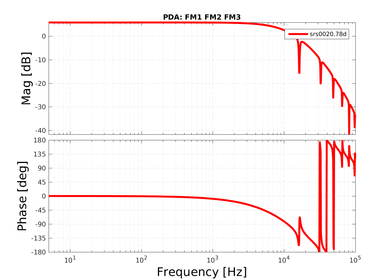
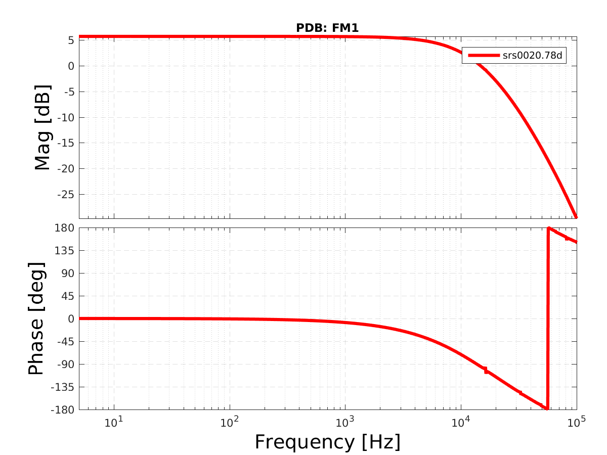
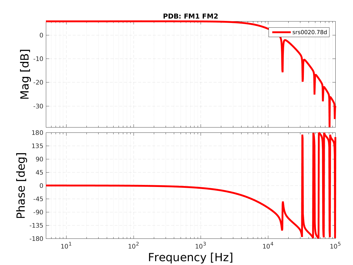
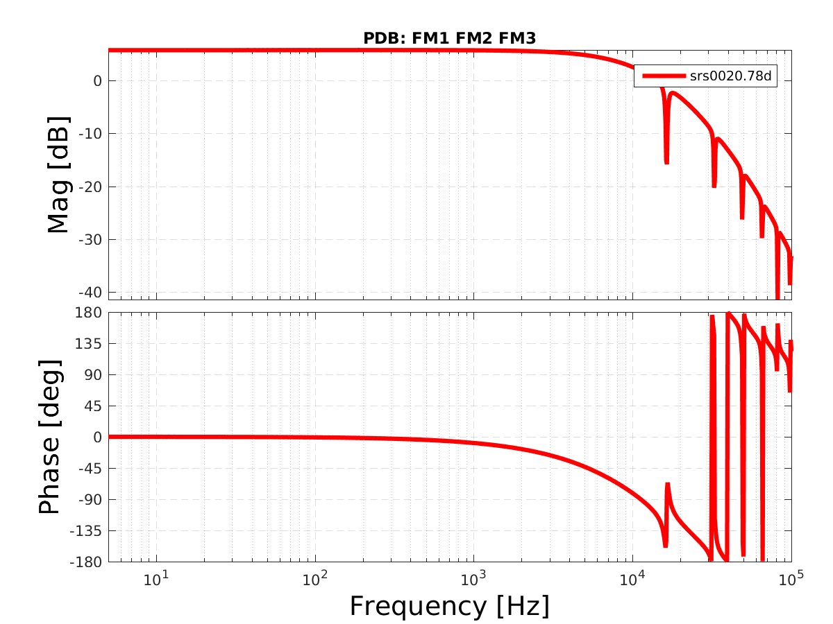
Updated the FM1,FM2,FM3 whitening compensation filters for PDA and PDB.
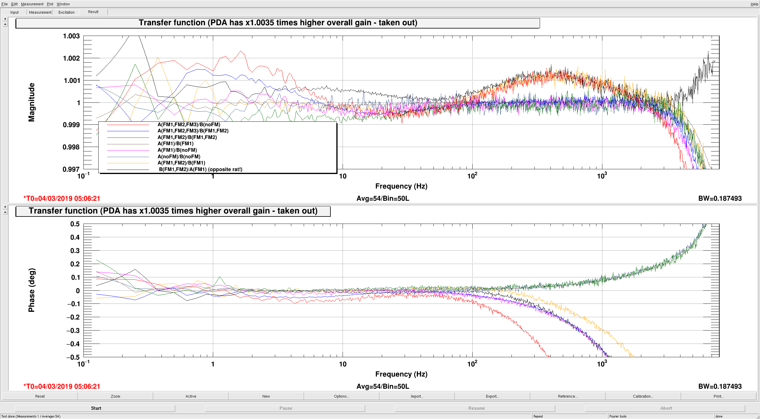
They are now matched at the +-0.15% level (see plot).
And we verified that they are no loner offset dependent.
Also, to be explicit: We disabled the 12dB, 6dB and 3dB whitening gain steps in both PDA and PDB. The 24dB step is still operational.
The new foton filters are:
PDA:
FM1: zpk([10.44],[0.996],0.9734,"n")
FM2: zpk([49.63],[497.5],-0.9995,"n")
FM3: zpk([10.372],[0.9865],1.002,"n")
PDB:
FM1: zpk([10.160],[0.969],0.975458,"n")
FM2: zpk([49.72],[497.7],-1.0004,"n")
FM3: zpk([10.467],[1.000],.9973,"n")
Using this filter, we injected pink noise into both DCPDs, and plotted the PD ratio in various configurations to verify the filter compensation. Specifically, plotted are:
A(FM1,FM2,FM3)/B(noFM)
A(FM1,FM2,FM3)/B(FM1,FM2)
A(FM1,FM2)/B(FM1,FM2)
A(FM1)/B(FM1)
A(FM1)/B(noFM)
A(noFM)/B(noFM)
A(FM1,FM2)/B(FM1)
B(FM1,FM2)/A(FM1) (opposite rat!)
The xml file with the data in the plot is in /ligo/home/controls/sballmer/20190303/DCPDfinal.xml
Finally, we still will have to re-match the photo diode light levels in lock (alog 47217).
All this was done to fix the problem identified in alog 47247.
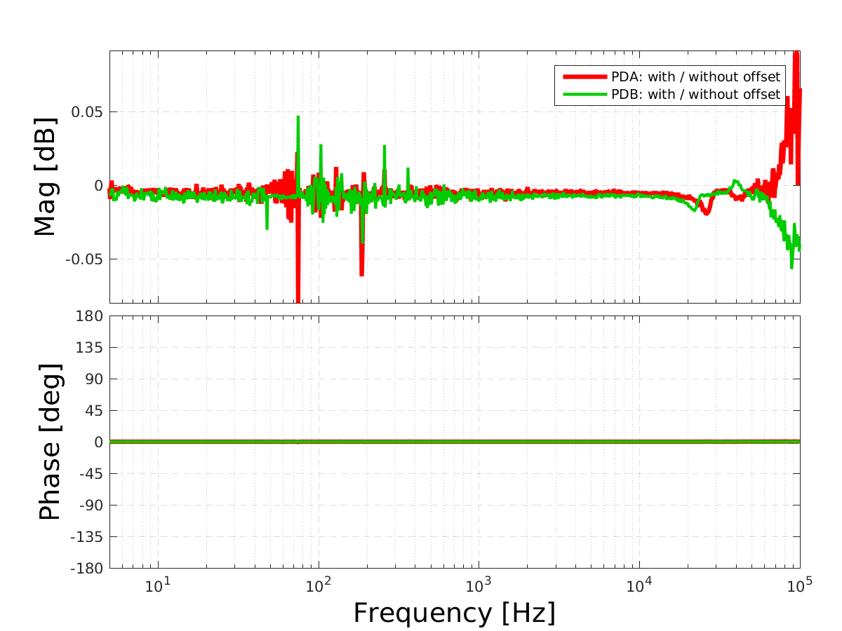
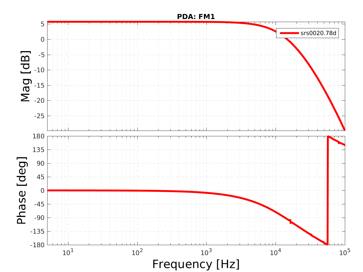
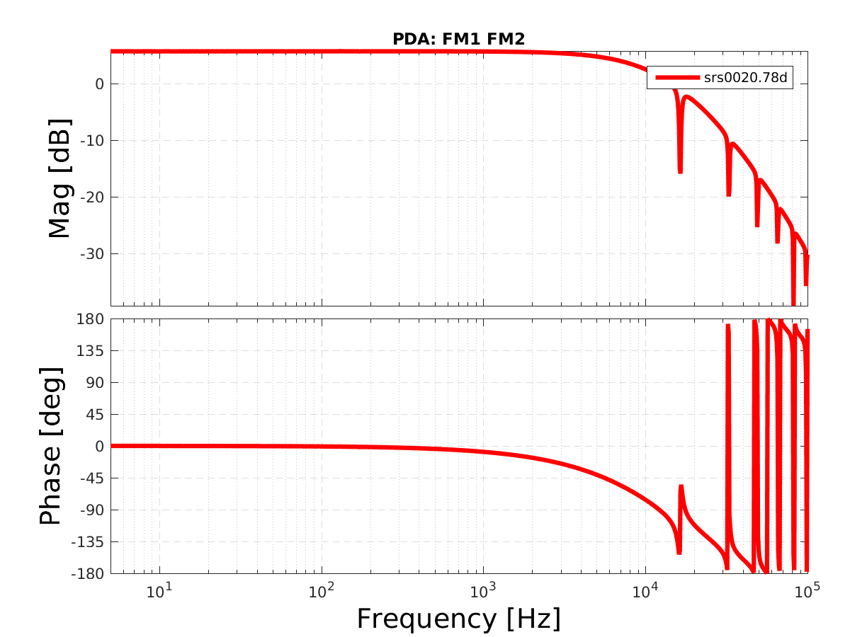
Attached are plots of
- Transfer function wit- over-without offset. The insanity is indeed gone.
- PDA: FM1, FM1FM2, FM1FM2FM3 - all normalized with their compensation filter.
- PDB: FM1, FM1FM2, FM1FM2FM3 - all normalized with their compensation filter.
In short: the current compensation is good at the 0.02dB level. One could still improve it...
The plotting MATLAB code is here: /ligo/home/controls/sballmer/20190304/DCPD
I've moved the contents of Stefan's results from his home directory on the local file system into the calibration SVN (though I've not yet modified his plotting script for the new directories and/or to spit out the right file names).
I used the follow commands to do so:
Data:
cd /ligo/svncommon/CalSVN/aligocalibration/trunk/Common/Electronics/H1/Data/OMCWhiteningChassis/2019-03-04/
cp /ligo/home/controls/sballmer/20190304/DCPD/SRS00* ./
cp /ligo/home/controls/sballmer/20190304/DCPD/srs00* ./
cp /ligo/home/controls/sballmer/20190304/DCPD/47254_20190303213* ./
Script:
cd /ligo/svncommon/CalSVN/aligocalibration/trunk/Common/Electronics/H1/Scripts/
cp /ligo/home/controls/sballmer/20190304/DCPD/plotData.m plot_omcdcpdwhiteningmods_20190304.m
Results:
cd /ligo/svncommon/CalSVN/aligocalibration/trunk/Common/Electronics/H1/Results/OMCWhiteningChassis/
cp /ligo/home/controls/sballmer/20190304/DCPD/PD*.png ./
rename 's/PD/2019-03-04\_H1OMC\_WhiteningChassisTFs\_PD/' PD*.png
Thus the new script name to plot the data is:
/ligo/svncommon/CalSVN/aligocalibration/trunk/Common/Electronics/H1/Scripts/plot_omcdcpdwhiteningmods_20190304.m
which should be modified to analyze the following data:
/ligo/svncommon/CalSVN/aligocalibration/trunk/Common/Electronics/H1/Data/OMCWhiteningChassis/2019-03-04/
SRS00*.78D
srs00*.asc
using the notes in the file
/ligo/svncommon/CalSVN/aligocalibration/trunk/Common/Electronics/H1/Data/OMCWhiteningChassis/2019-03-04/
47254_20190303213544_DCPDWhiteningChanges.pdf
and to produce plots and results with similar file tags as
/ligo/svncommon/CalSVN/aligocalibration/trunk/Common/Electronics/H1/Results/OMCWhiteningChassis/
2019-03-04_H1OMC_WhiteningChassisTFs_PD*.png
(or the code should be re-written to use your favorite fitting code [maybe in python using IIRrational] and produce plots and results with similarly explicit file names with indications of the date, the interferometer, and WhiteningChassisTFs in the file name.)
Lilli S.,
First, I have renamed the data files in dir /ligo/svncommon/CalSVN/aligocalibration/trunk/Common/Electronics/H1/Data/OMCWhiteningChassis/2019-03-04/, so that they match what is described in note /ligo/svncommon/CalSVN/aligocalibration/trunk/Common/Electronics/H1/Data/OMCWhiteningChassis/2019-03-04/47254_20190303213544_DCPDWhiteningChanges.pdf
The test box has been factored out. (Test box data: /ligo/svncommon/CalSVN/aligocalibration/trunk/Common/Electronics/H1/Data/CoilDriverTestBox/S1900070/)
The fitting script is /ligo/svncommon/CalSVN/aligocalibration/trunk/Common/Electronics/H1/Scripts/fit_OMCDCPDWhiteningChassis_20190304.py
The results are in the table below. The fitting plots are in the attachments.
The low-freq poles/zeros roughly match Stefan's results. In O1 and O2 we used 1 stage of whitening (FM1), and the high freq poles were at [(14.34e3 + 14.60e3)/2, (18.68e3 + 18.57e3)/2, (98.94e3 + 100.45e3)/2] Hz. The new fitting for FM1 is consistent with O1 and O2.
Take PDA FM1FM2FM3 noDC as an example, manually build TF by removing the high-freq zeros, and plot the residual -> see diff.pdf
By ignoring the high-freq zeros, there's little impact on magnitude, but there's phase difference at higher freq (~<1 deg below 5k Hz).
| PDA | PDB | Comments | |
| FM1FM2FM3 (no DC) | PDA, Filters: FM1FM2FM3noDC Results: z:p:k [ 3.90426349e+06 3.90426349e+06 4.99892253e+02 1.08290122e+00 1.08040698e+00] [ 1.04233314e+01 3.26866242e+04 3.26866242e+04 1.13980014e+04 4.97078295e+01 1.04233314e+01] -8.68011786846 |
PDB, Filters: FM1FM2FM3noDC Results: z:p:k [ 4.64029327e+06 4.64029327e+06 5.00447159e+02 1.07523773e+00 1.07282309e+00] [ 1.03389750e+01 3.28642175e+04 3.28642175e+04 1.15193027e+04 1.03389750e+01 4.97939024e+01] -6.26981682358 |
Low-freq zeros near 1Hz, 1Hz, 500Hz, and poles near 10Hz, 10Hz, 50Hz (as expected) High-freq poles near 12K, 33K, 33K Hz. |
| FM1FM2FM3 (4.99V DC) | PDA, Filters: FM1FM2FM3DC Results: z:p:k [ 4.83659991e+06 4.83659991e+06 4.99682906e+02 1.08106936e+00 1.08299624e+00] [ 1.04231076e+01 3.28748478e+04 3.28748478e+04 1.13460627e+04 1.04231076e+01 4.96890494e+01] -5.6929144981 |
PDB, Filters: FM1FM2FM3DC Results: z:p:k [ 3.93271594e+06 3.93271594e+06 5.00449636e+02 1.07585358e+00 1.07328174e+00] [ 4.98000266e+01 3.28631506e+04 3.28631506e+04 1.15205406e+04 1.03375026e+01 1.03375026e+01] -8.72188264417 |
Low-freq zeros near 1Hz, 1Hz, 500Hz, and poles near 10Hz, 10Hz, 50Hz (as expected) High-freq poles near 12K, 33K, 33K Hz. |
| FM1FM2 (no DC) |
PDA, Filters: FM1FM2 Results: z:p:k |
PDB, Filters: FM1FM2 Results: z:p:k [ 2.11805525e+06 8.72055868e+05 5.00733633e+02 1.14755102e+00] [ 2.04506589e+04 1.24360067e+04 8.94998324e+04 4.97729997e+01 1.02056871e+01] -12.7328787001 |
Low-freq zeros near 1Hz, 500Hz, and poles near 10Hz, 50Hz (as expected) High-freq poles near 12K, 20K, 89K Hz. |
| FM1 (no DC) | PDA, Filters: FM1 Results: z:p:k [ 4.22938089e+06 4.22938089e+06 1.17507390e+00] [ 1.27384958e+04 1.93716076e+04 9.29113659e+04 1.04895576e+01] 13.3497796427 |
PDB, Filters: FM1 Results: z:p:k [ 4.84207436e+06 4.84207436e+06 1.14699930e+00] [ 1.29122349e+04 1.93696499e+04 9.46279852e+04 1.02067553e+01] 10.4974545401 |
Low-freq zeros near 1Hz and poles near 10Hz (as expected) High-freq poles near 13K, 19K, 93K Hz. |
| noFM (no DC) | PDA, Filters: noFM Results: z:p:k [ 1.26091781e+07 3.57048935e+07 2.05610666e-01] [ 1.28075383e+04 1.92624890e+04 1.84656469e+06 4.98134421e-02] 0.980629117874 |
PDB, Filters: noFM Results: z:p:k [ 2.82948542e+07 2.84161583e+07 2.05615042e-01] [ 1.29617754e+04 1.93273505e+04 2.08761329e+06 4.98133861e-02] 0.629314166113 |
High-freq poles near 13K, 19K Hz. Unphysical low-freq zero near 0.2Hz and pole near 0.05Hz. |
Concluding from the results of the fit above, I'll be updating the calibration model parameters to change from the previous measurement of the DCPD whitening chassis (before O2, when the nominal configuration was to only have the first stage of whitening -- "F1" or "FM1" -- on; see LHO aLOG 28087) from PDA PDB PDA PDB PDA PDB uncompOMCpoles_whitening = [(14.34e3 + 14.60e3)/2, (18.68e3 + 18.57e3)/2, (98.94e3 + 100.45e3)/2]; to the new fitted measurement results, and choosing the new nominal configuration, with all three filters on (the 1st and 3rd stages, which are whitening and the 2nd stage which is a low pass, i.e. "FM1FM2FM3" or "3 filt"), and using the 5 V_DC offset fit results because it's more representative of the nominal running conditions of the chassis (with the poles rounded to the nearest Hz) PDA PDB PDA PDB PDA PDB uncompOMCpoles_whitening = [(11.346e3 + 11.521e3)/2, (32.875e3 + 32.863e3)/2, (32.875e3 + 32.863e3)/2];
Lilli S.,
The residual contribution plot is attached. This was generated using /ligo/svncommon/CalSVN/aligocalibration/trunk/Common/Electronics/H1/Scripts/fit_OMCDCPDWhiteningChassis_20190304-vsOriginal.py
(based on reference model modelparams_H1_20190118)
The results is averaged after using different poles/zeros in PDA and PDB, instead of using the same set of averaged poles/zeros in PDA and PDB.
Per Jeff's request that the original DCPD files be included, I am attaching the data extending down to 0.5Hz for the OMC DCPD Whitening chain as taken on the floor by signal injection into the front panel of the Split Whitening Chain via an SR785
Attached are two plots:
A) The comparison of TFs:
1. All low-freq z:p + high-freq p + out-of-band z from IIRrational fitting
2. Dead reckoned z:p = [500, 1, 1]:[50, 10, 10]
3. Low-freq z:p from Stefan's fitting in 47257
4. Low-freq z:p from Stefan's fitting in 47257 + high-freq p from IIRational
B) The comparison of contribution residuals, by using the latest H1 model 20190301
The scripts live in
/ligo/svncommon/CalSVN/aligocalibration/trunk/Common/Electronics/H1/Scripts/fit_OMCDCPDWhiteningChassis_20190304-compareTF.py
/ligo/svncommon/CalSVN/aligocalibration/trunk/Common/Electronics/H1/Scripts/fit_OMCDCPDWhiteningChassis_20190304-compareRes.py
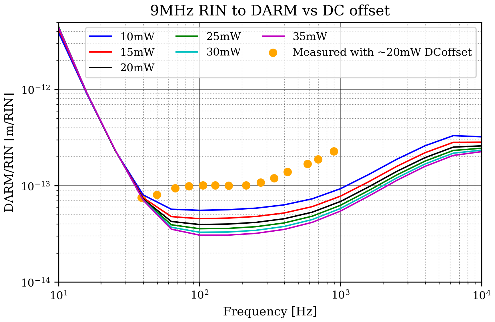
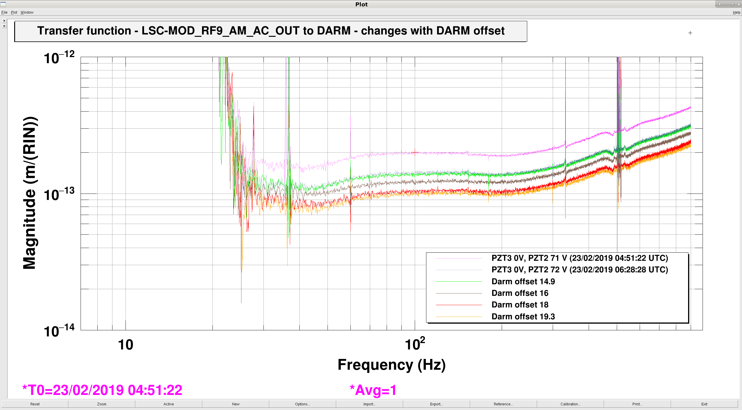
I have been looking at the 9MHz RIN coupling to DARM in a Finesse model to see how it compares to the measurements done in alog 47243. In particular I was interested in the shape and its dependence on the DARM offset.
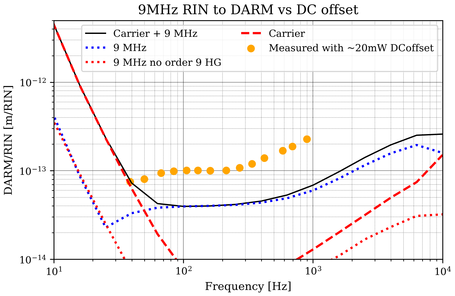
In summary: the model suggest that what we are measuring is the 9th order HG mode of the 9MHz coupling through the OMC.
Modulating the 9MHz modulation index results in both the 9 and carrier being amplitude modulated. Modelling the transfer function dependence on DARM offset (Quantified in DC power at OMC DCPDs) produces this:

Breaking down the various terms of the coupling we see:

The carrier coupling term does not change with DARM offset, the 9MHz does. Also plotted is the 9MHz coupling with the 9th order modes removed. The 9th order terms are the dominant at high frequency. The shape also appears to match the broadband injections, reducing below 100Hz.
If the individual couplings terms are to be believed the carrier term is actually much less than modelled, whereas the 9Mhz 9th order is greater. The latter will depend on the position of the beam relative to the point absorbers which I haven't explored yet. Why the carrier term would be much lower in the measurements I am currently unsure.
We can also plot how the 9th order 9MHz coupling drops with DARM offset, looks like it is 1/sqrt(DCPD power) or equivalently 1/(DARM offset) from the model. Which is the lower residual fit that Craig tried.

The model contained:
The 1/DARM_offset of 1/sqrt(DCPD) coupling can be explained by considering a CONSTANT amount of 9MHz HOM coupling to the DCPDs, while the optical gain scales with the offset, such that the same amount of 9MHz RIN at the DCPD is interpreted as a different noise level in m/rHz.
We have been taking some ASC measurements while locked on RF DARM for DCPD whitening investigations.
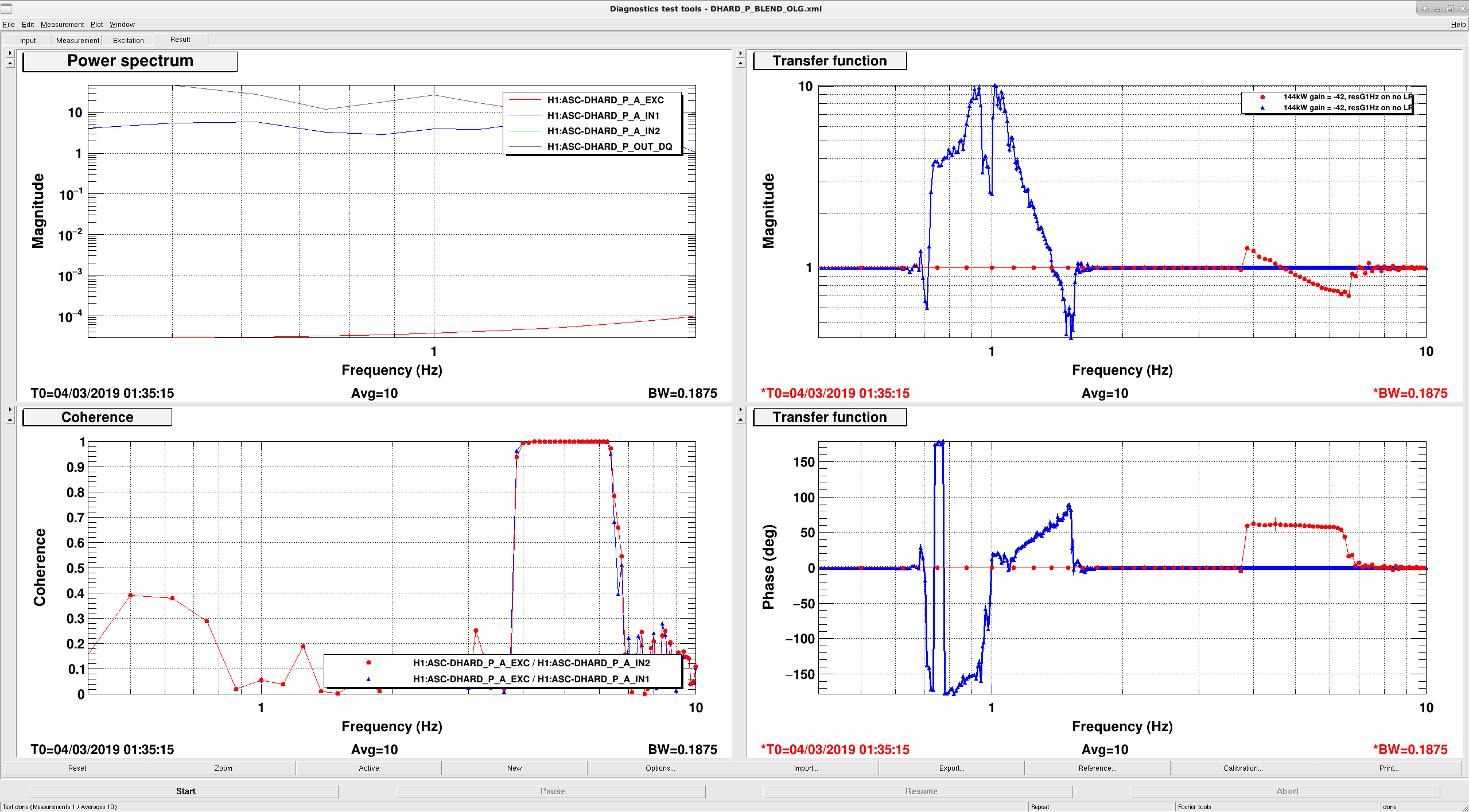
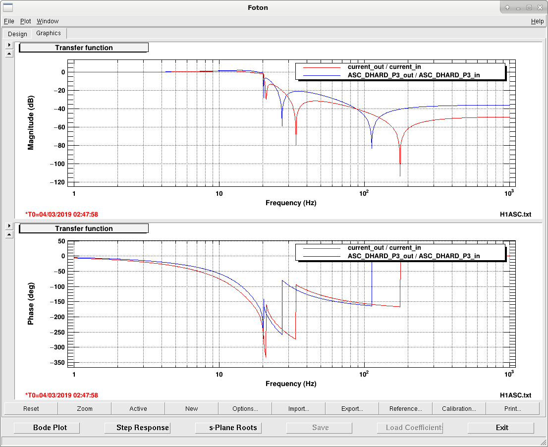
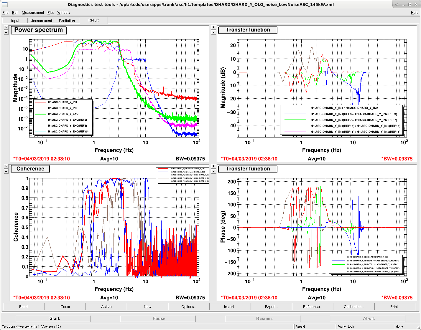
It seems that lowering the DHARD P gain by a factor of 2 (47232 ) was causing a 1 Hz instability yesterday and Friday night. We made some measurements of the DHARD loop in the low noise ASC state, the attached screenshot shows the measurement with the 1 Hz resG engaged, the gain at -42 and no low pass engaged. We still have the non-minimum phase at 1 Hz, and if we were to reduce the gain to -21 as we did on friday this would be very close to unstable. Instead of trying to reduce the gain, we decided to just modify the low pass filter. We modified the ELP10b filter (FM1) to be a 20Hz low pass which gives us a bit more roll off that the ELP17Hz which was for this measurement of the noise in DARM (both are shown in the second attachment). The guardian will now leave the gain of DHARD Y at -42, and turn on the new 20Hz low pass. This seems to be a sort of OK compromise between gain peaking at 5 Hz and at 1 Hz.
For DHARD Y, the filter gain hasn't changed at high frequency, but the combination of 2 low pass filters that we were using wasn't very good. The forth attachment shows the new ELP20 filter that I swapped out for the old cut off, it gives us back about 10 degrees of phase at the 4Hz ugf and gives us about a factor of 3 less control signal around 35Hz. In the guardian I have swapped FM2+8 for FM9.
We haven't been able to test these changes.
Craig, Rich, Peter, Stefan,
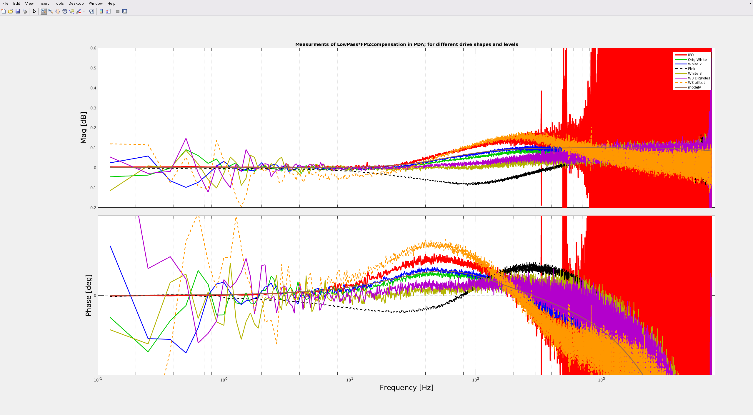
We tried to measure and fine-tune the DCPD whitening filter compensation. so we took the following measurments:
a) Analog transfer function on the floor for PDA & PDB; FM1FM2FM3 all off and FM1FM2FM3 all on (run configuration). (That's 4 measurements total.) That data is still on disk and Rich will post it.
b) Driving both DCPDs with noise, measure the PDA/PDB transfer function. This is done with FM1&FM2 on PDA and FM1 on PDB, normalized by FM1 on PDA and FM1 on PDB to take out other systematics.
Measurement b) was performed with a variety of noise sources:
i) IFO on AS_RF45, with additional 100Hz-1kHz frequency noise injection. (IFO)
ii) White noise drive (10Vpkk) (Orig white)
iii) Same white noise, but FM6 filters in PDA and PDB off (White 2). Note that changed the transfer function at the 1e-3 level compared with ii) - consistent with T990013-B (dtt documentation)
iv) Same white noise, but now filtered by SR560 with 2 poles at 100Hz (Pink)
v) White noise at half the level (5Vpkk) (White 3)
vi) Same as white 3, but with 2 poles at 100Hz in the digital system (W3 Dig Poles)
vii) Same as white 3, but additional 2V offset (~13000cts at IN1) (W3 offset)
viii) Simple model z59.8265:p60.174,120k
Note that at 100Hz the transfer function is changing by as much as 0.3dB (3.5%) with drive level..THis is much bigger than the expected dtt error, so we conclude it is real, We will deal with the implications for calibration tomorrow.
I attach the data taken with the SR785 on the DCPD Whitening chain.
Problem fixed in alog 47254.
I opened (and subsequently closed) FRS Ticket 12453 that corresponds to this issue. As Stefan mentions, the solution has already been implemented (and will likely become an ECR to change all OMC DCPD whitening chassis).
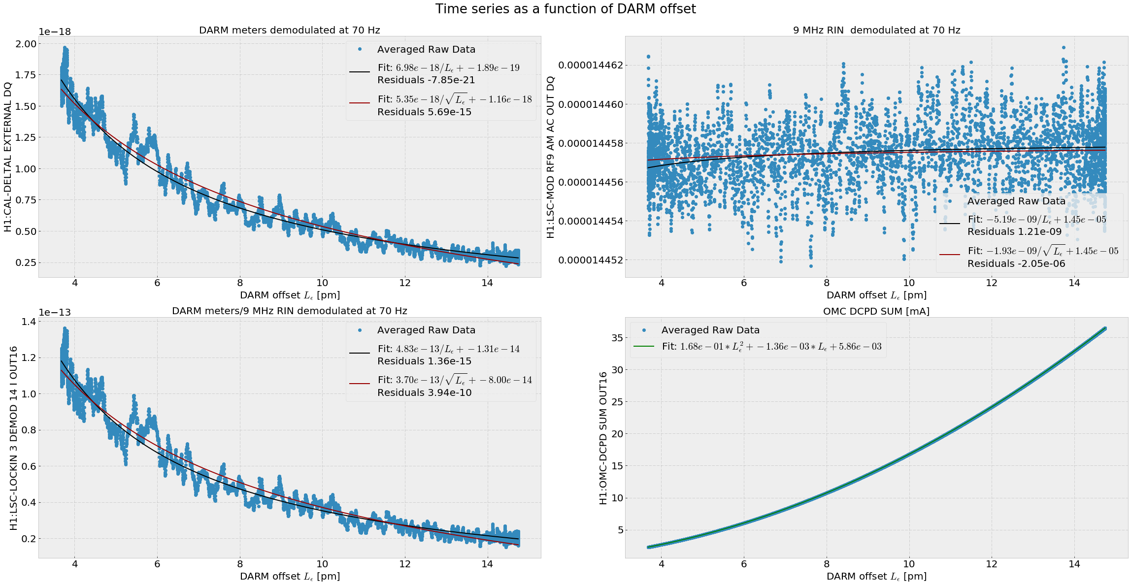
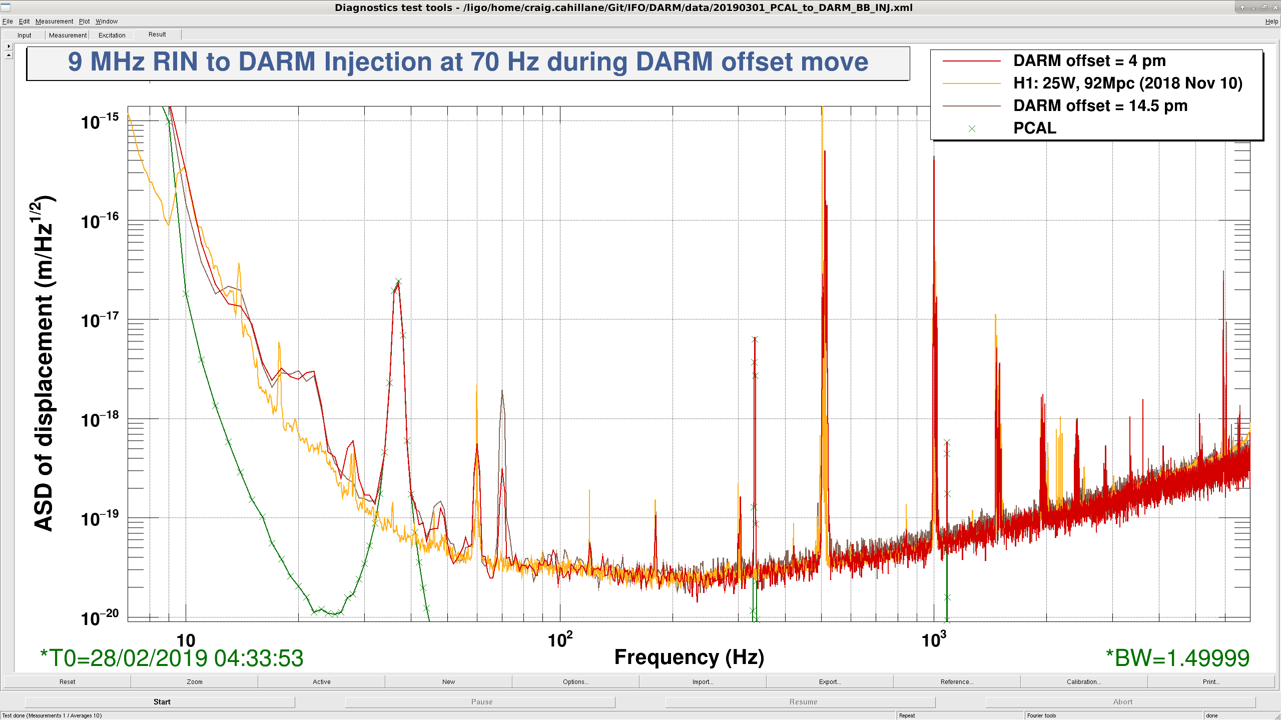
A while ago Georgia and I moved the DARM offset and found that the 9 MHz RIN to DARM coupling decreases with increasing DARM offset. Two days ago, I swept the DARM offset from 4 pm to 14.7 pm while a 70 Hz 9 MHz RIN line was on and present in DARM. I then demodulated the line in software, plotted it as a function of DARM offset, and compared a few models to the data. It seems that 9 MHz RIN to DARM coupling falls like 1/DARM offset. This rules out couplings like those explained by Kiwamu in attachment 4, which increase with increased DARM offset.
The 1/DARM_offset of 1/sqrt(DCPD) coupling can be explained by considering a CONSTANT amount of 9MHzHOM coupling to the DCPDs, while the optical gain scales with the offset, such that the same amount of 9MHz RIN at the DCPD is interpreted as a different noise level in m/rHz.