|
Work Permit |
Date |
Description |
alog/status |
|
6363.html |
2016-11-29 14:14 |
change IFO node to disallow SDF diffs in the decision for observation mode. Review current exceptions list prior to O2. |
|
|
6362.html |
2016-11-29 09:54 |
Replace POP90 demod chassis. See alog 31948. |
31971 |
|
6361.html |
2016-11-29 08:59 |
Reconfigure power to the Vault equipment to provide +-12Vdc instead of just +12. Power up equipment and get signals to MidX |
|
|
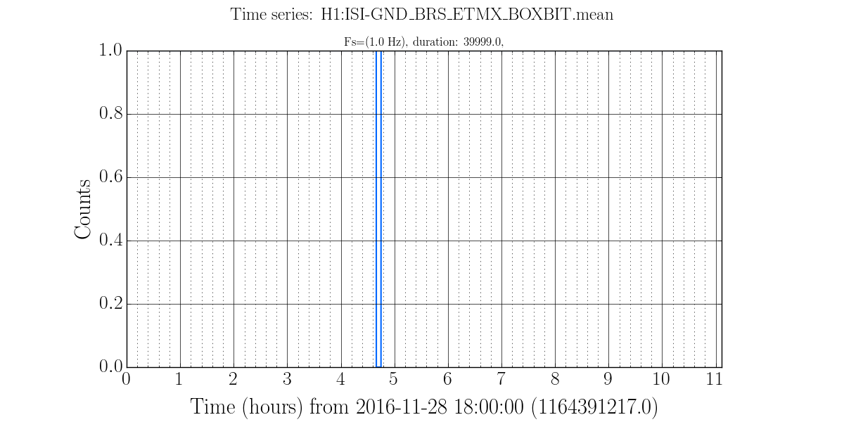
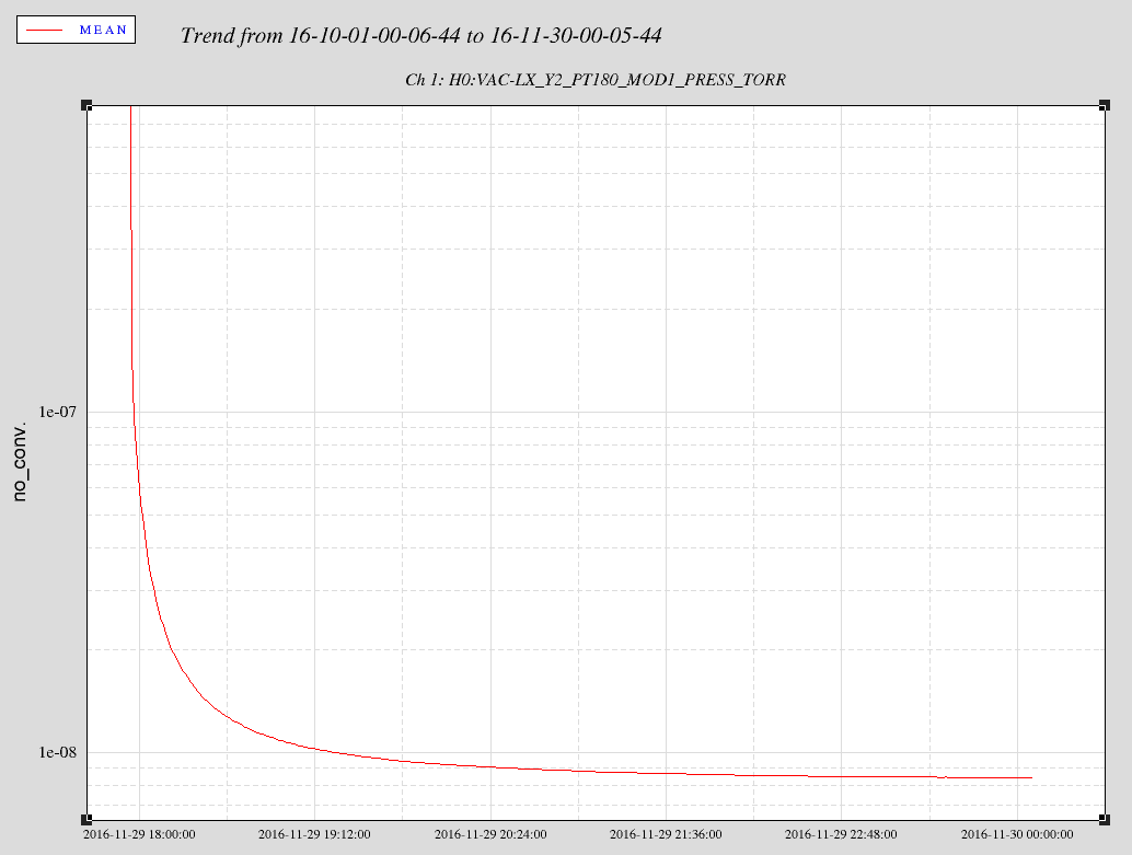
6360.html |
2016-11-29 08:16 |
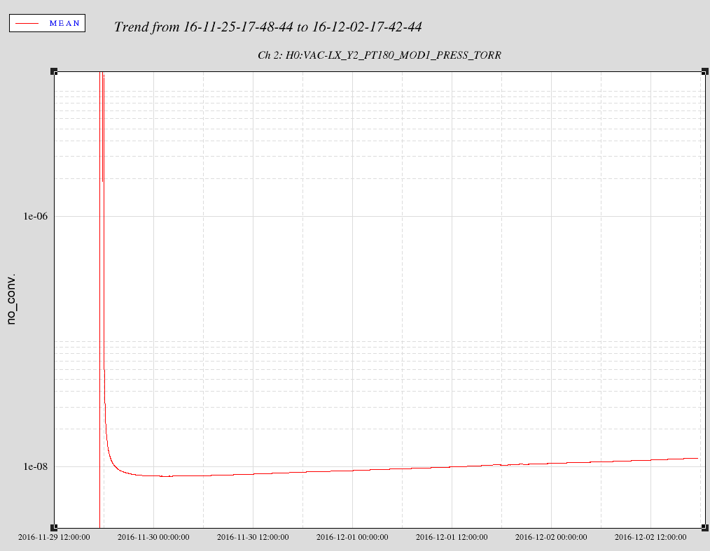
Connect electronics to PT180 sensor tube and energize*Open isolation valve to expose PT180 to site vacuum volume*vent locally mounted turbo, remove and replace it with 1 1/2" O-ring valve + nominal 2.75"CF-NW40 adapter*Pump to rough vacuum the volume between in-series 1 1/2" pump port valves |
31970 |
|
6359.html |
2016-11-29 06:41 |
Tour AREVA group (~8) around site, including LVEA. |
|
|
6358.html |
2016-11-28 17:33 |
Update vacuum alarm handler at ops station: Add _ERROR channels for all existing channels. Add all pressure gauges. Remove all commented out channels except CP3. Update guidance text. |
31965 |
|
6357.html |
2016-11-28 16:09 |
For each Vacuum channel being monitored by the cell phone texter, also monitor the corresponding ERROR channel and alarm any errors are non-zero. |
|
|
6356.html |
2016-11-28 14:55 |
Change displays in control room in preparation for O2. Add DARM BLRMS to Video0 (sharing with ASC Err sigs). Remove SDF overview screen from Video0 (information is already redundant with newly updated CDS overview screen). Ensure templates are linked to userapps repo, so that most up-to-date FOM is displayed upon computer reboot. |
|
|
6355.html |
2016-11-28 14:10 |
Install RF Amplifiers (ZHL-1A+) to add gain to the indoor PEM antenna signals from CER/LVEA. |
31928 |
|
6354.html |
2016-11-28 11:48 |
Remove BP_IN1 channels from DAQ list in h1susprocpi for modes not being actively damped (all except modes 3, 26, 27, 28) |
31927 |
|
6353.html |
2016-11-28 11:36 |
ECR1600351, add 41 fast DQ channels to H1BROADCAST0.ini, restart dmt-broadcaster. |
31927 |
|
6352.html |
2016-11-28 10:56 |
Update Matlab license, there will be a 15 minutes interruption on Matlab. |
WP#6352 & WP#6351 are duplicates |
|
6351.html |
2016-11-28 10:56 |
Update Matlab license, there will be a 15 minutes interruption on Matlab. |
|
|
6350.html |
2016-11-28 10:10 |
Remove some channels from the frame to save data rate. h1alsex: Remove H1:LSC-X_EXTRA_AI channels from the commissioning frame. No need to archive. h1alsey: Same as h1alsex. h1lsc: Remove H1:LSC-JITTERFF_OUT from the commissioning frame. This feature is not used for now and no need to archive. |
31927 |
|
6349.html |
2016-11-28 10:01 |
Investigate communication issues withing Beckhoff that began when Kyle powered down PT180 |
|
|
6348.html |
2016-11-28 10:00 |
Adjust the laser power on the ETMx and ETMy oplev lasers in an attempt to fix the ongoing laser glitches. |
31909 |
|
6347.html |
2016-11-28 09:54 |
Forklift PSL backup chiller from Mechanical building to OSB receiving. |
|
|
6346.html |
2016-11-28 08:21 |
Update the calibration code to gstlal-calibration-1.0.9-v1, fix bugs, apply calibration factors, and apply new filters: * Update calib_state_vector calculation to better accommodate changes in kappa smoothing. * Add check for overflow input to GDS pipeline. * Apply the real parts of kappa_tst, kappa_pu, and kappa_c at LHO. * Update the calibration filter file as needed. |
31926 & 31924 |
|
6345.html |
2016-11-25 14:42 |
Replace piezo mirror mount on PSL table. This is the implementation of E1500404 and FRS4639. The work may or may not be done: alignment and PEM injections are higher priority. Approved by Keita. |
31935 & 31974 |

For completeness, here are the guardian nodes which are currently excluded from the decision of whether to go/stay in observation mode:
EXCLUDE_NODES = [
'DIAG_MAIN',
'INJ_TRANS',
'VIOLIN_DAMPER',
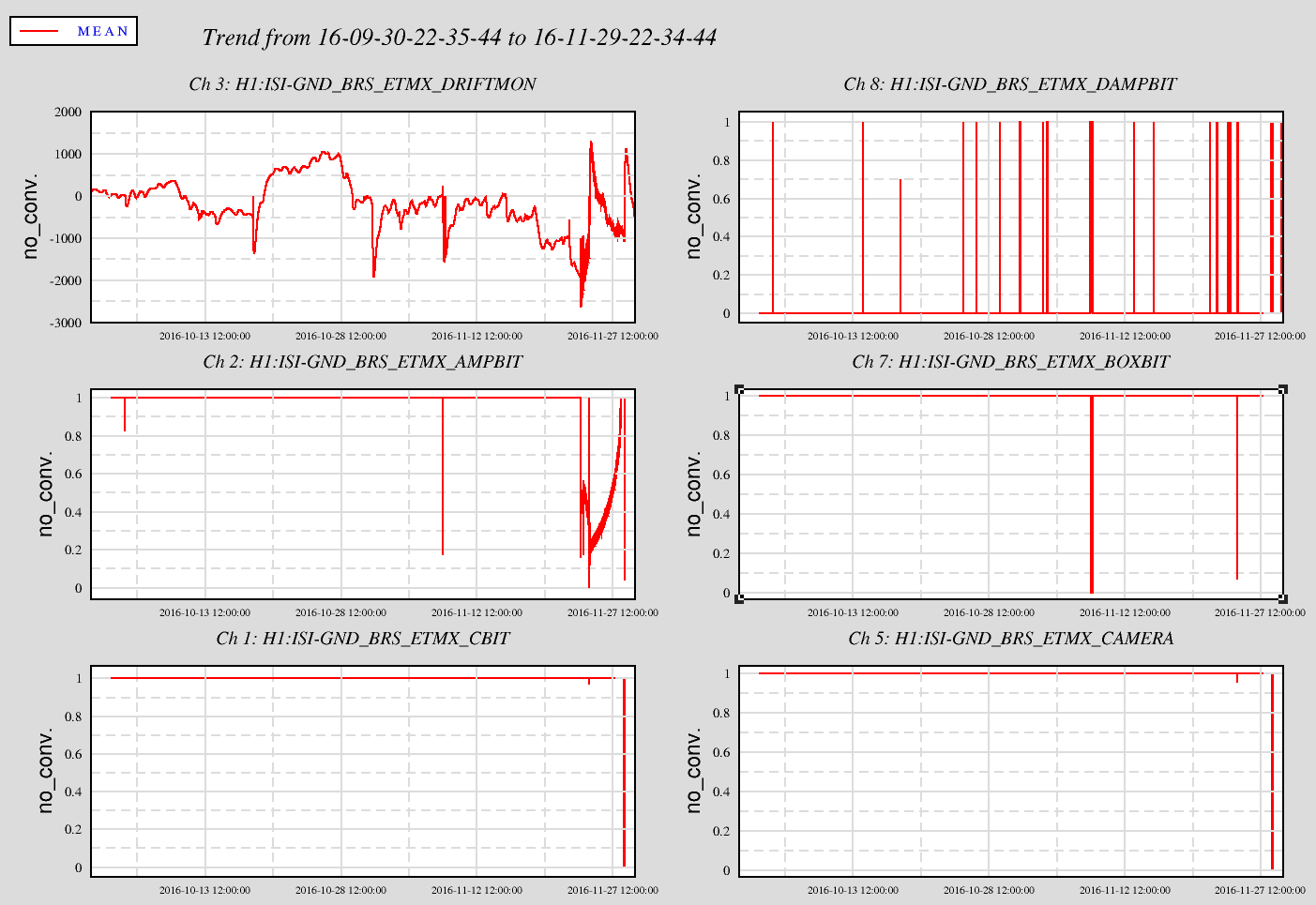
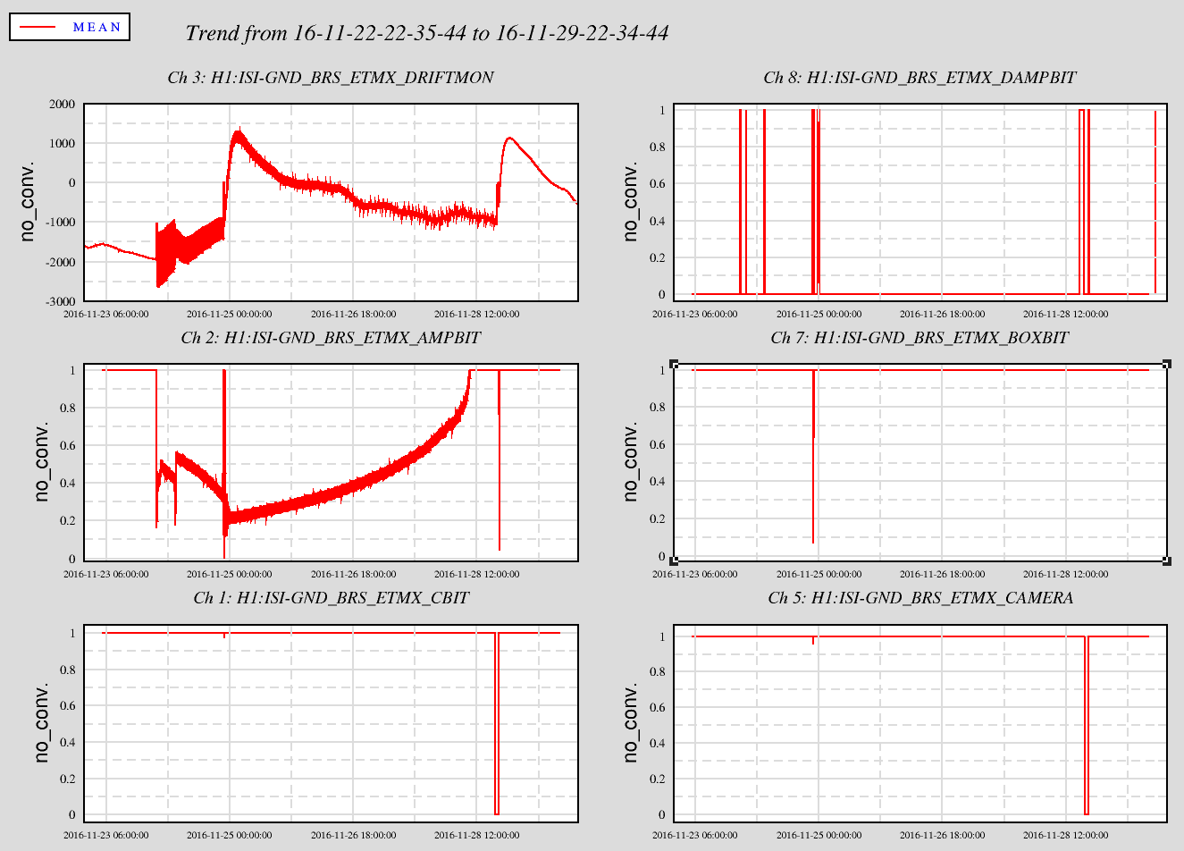
'BRSX_STAT',
'BRSY_STAT',
'CS_BRS',
]
Also excluded are all Seismic CONF nodes and the IFO node itself.
Code is: /opt/rtcds/userapps/release/sys/h1/guardian/IFO_NODE_LIST.py
This file is only used by the IFO guardian node.